MC74LCX06DTG ON Semiconductor, MC74LCX06DTG Datasheet
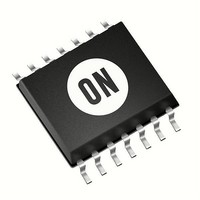
IC INVERTER HEX LV CMOS 14-TSSOP

MC74LCX06DTG

Manufacturer Part Number
MC74LCX06DTG
Description
IC INVERTER HEX LV CMOS 14-TSSOP
Manufacturer
ON Semiconductor
Series
74LCXr
Datasheet

Specifications of MC74LCX06DTG

Logic Type
Inverter with Open Drain
Number Of Inputs
1
Number Of Circuits
6
Current - Output High, Low
24mA, 24mA
Voltage - Supply
2 V ~ 3.6 V
Operating Temperature
-40°C ~ 85°C
Mounting Type
Surface Mount
Package / Case
14-TSSOP
Logic Family
LCX
Number Of Channels Per Chip
5
Polarity
Inverting
Supply Voltage (max)
3.6 V
Supply Voltage (min)
2 V
Maximum Operating Temperature
+ 85 C
Mounting Style
SMD/SMT
Low Level Output Current
24 mA
Minimum Operating Temperature
- 40 C
Number Of Lines (input / Output)
6 / 6
Output Type
Open Drain
Propagation Delay Time
4.1 ns at 2.7 V, 3.7 ns at 3.3 V
Lead Free Status / RoHS Status
Lead free / RoHS Compliant
MC74LCX06
Low−Voltage CMOS Hex
Inverter with Open Drain
Outputs
With 5 V − Tolerant Inputs
from a 2.3 V to 3.6 V supply. High impedance TTL compatible inputs
significantly reduce current loading to input drivers. These LCX
devices have open drain outputs which provide the ability to set output
levels, or do active−HIGH AND or active−LOW OR functions. A V
specification of 5.5 V allows MC74LCX06 inputs to be safely driven
from 5.0 V devices.
Features
*For additional information on our Pb−Free strategy and soldering details, please
January, 2005 − Rev. 7
download the ON Semiconductor Soldering and Mounting Techniques
Reference Manual, SOLDERRM/D.
The MC74LCX06 is a high performance hex inverter operating
System Power Requirements
Device
Designed for 2.3 V to 3.6 V V
5.0 V Tolerant Inputs/Outputs
LVTTL Compatible
LVCMOS Compatible
24 mA Output Sink Capability
Near Zero Static Supply Current (10 mA) Substantially Reduces
Latchup Performance Exceeds 500 mA
Wired−OR, Wired−AND
Output Level Can Be Set Externally Without Affecting Speed of
Functionally Compatible with LCX05
ESD Performance:
Pb−Free Packages are Available*
Semiconductor Components Industries, LLC, 2005
Figure 1. Pinout: 14−Lead (Top View)
V
A0
14
CC
1
O0
A3
13
2
A1
O3
12
3
Human Body Model >1500 V;
Machine Model >200 V
O1
A4
11
4
O4
A2
CC
10
5
Operation
O2 GND
A5
9
6
O5
8
7
1
I
14
See detailed ordering and shipping information in the package
dimensions section on page 2 of this data sheet.
14
14
1
1
1
ORDERING INFORMATION
A
WL, L
Y
WW, W = Work Week
http://onsemi.com
CASE 751A
CASE 948G
SOEIAJ−14
DT SUFFIX
TSSOP−14
CASE 965
D SUFFIX
M SUFFIX
SOIC−14
= Assembly Location
= Wafer Lot
= Year
Publication Order Number:
14
1
14
14
1
1
DIAGRAMS
MARKING
74LCX06
MC74LCX06/D
AWLYWW
ALYW
ALYW
LCX06
LCX
06

Related parts for MC74LCX06DTG

MC74LCX06DTG Summary of contents

Page 1

... Figure 1. Pinout: 14−Lead (Top View) *For additional information on our Pb−Free strategy and soldering details, please download the ON Semiconductor Soldering and Mounting Techniques Reference Manual, SOLDERRM/D. Semiconductor Components Industries, LLC, 2005 January, 2005 − Rev GND 1 http://onsemi.com MARKING DIAGRAMS 14 SOIC−14 ...

Page 2

Figure 2. Logic Diagram MAXIMUM RATINGS Symbol Parameter V DC Supply Voltage Input Voltage ...

Page 3

RECOMMENDED OPERATING CONDITIONS Symbol V Supply Voltage CC V Input Voltage I V Output Voltage O I LOW Level Output Current OL Sink T Operating Free−Air Temperature A Dt/DV Input Transition Rise or Fall Rate ELECTRICAL CHARACTERISTICS Symbol ...

Page 4

Vmi An t PZL On Vmo PROPAGATION DELAYS 2.5 ns, 10 MHz Table 3. AC WAVEFORMS 3 0.3 V Symbol V 1 1.5 ...

Page 5

G −T− SEATING 14 PL PLANE 0.25 (0.010 14X REF 0.10 (0.004) 0.15 (0.006 L PIN 1 IDENT. 1 0.15 (0.006) T ...

Page 6

... E L DETAIL P VIEW American Technical Support: 800−282−9855 Toll Free USA/Canada Japan: ON Semiconductor, Japan Customer Focus Center 2−9−1 Kamimeguro, Meguro−ku, Tokyo, Japan 153−0051 Phone: 81−3−5773−3850 http://onsemi.com 6 NOTES: 1. DIMENSIONING AND TOLERANCING PER ANSI Y14.5M, 1982. ...

Related keywords