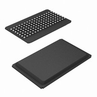
CY7C1370D-200BGXC Cypress Semiconductor Corp, CY7C1370D-200BGXC Datasheet - Page 10

CY7C1370D-200BGXC
Manufacturer Part Number
CY7C1370D-200BGXC
Description
IC SRAM 18MBIT 200MHZ 119BGA
Manufacturer
Cypress Semiconductor Corp
Type
Synchronousr
Specifications of CY7C1370D-200BGXC
Memory Size
18M (512K x 36)
Package / Case
119-BGA
Format - Memory
RAM
Memory Type
SRAM - Synchronous
Speed
200MHz
Interface
Parallel
Voltage - Supply
3.135 V ~ 3.6 V
Operating Temperature
0°C ~ 70°C
Access Time
3 ns
Maximum Clock Frequency
200 MHz
Supply Voltage (max)
3.6 V
Supply Voltage (min)
3.135 V
Maximum Operating Current
300 mA
Maximum Operating Temperature
+ 70 C
Minimum Operating Temperature
0 C
Mounting Style
SMD/SMT
Number Of Ports
4
Operating Supply Voltage
3.3 V
Lead Free Status / RoHS Status
Lead free / RoHS Compliant
Lead Free Status / RoHS Status
Lead free / RoHS Compliant, Lead free / RoHS Compliant
Available stocks
Company
Part Number
Manufacturer
Quantity
Price
Company:
Part Number:
CY7C1370D-200BGXC
Manufacturer:
Cypress Semiconductor Corp
Quantity:
10 000
Truth Table
The Truth Table for CY7C1370D and CY7C1372D follows
Notes
Document Number: 38-05555 Rev. *H
Deselect Cycle
Continue Deselect Cycle
Read Cycle (Begin Burst)
Read Cycle (Continue Burst)
NOP/Dummy Read (Begin Burst)
Dummy Read (Continue Burst)
Write Cycle (Begin Burst)
Write Cycle (Continue Burst)
NOP/Write Abort (Begin Burst)
Write Abort (Continue Burst)
Ignore Clock Edge (Stall)
Sleep Mode
1. X = “Don't Care”, H = Logic HIGH, L = Logic LOW, CE stands for ALL Chip Enables active. BWx = L signifies at least one Byte Write Select is active, BWx = Valid
2. Write is defined by WE and BW
3. When a write cycle is detected, all I/Os are tristated, even during byte writes.
4. The DQ and DQP pins are controlled by the current cycle and the OE signal.
5. CEN = H inserts wait states.
6. Device will power-up deselected and the I/Os in a tristate condition, regardless of OE.
7. OE is asynchronous and is not sampled with the clock rise. It is masked internally during write cycles.During a read cycle DQ
signifies that the desired byte write selects are asserted, see Write Cycle Description table for details.
inactive or when the device is deselected, and DQ
Operation
X
. See Write Cycle Description table for details.
None
None
External
Next
External
Next
External
Next
None
Next
Current
None
Address
Used
s
= data when OE is active.
CE
H
X
L
X
L
X
L
X
L
X
X
X
.[1, 2, 3, 4, 5, 6, 7]
ZZ
H
L
L
L
L
L
L
L
L
L
L
L
ADV/LD
H
H
H
H
H
X
X
L
L
L
L
L
WE
H
H
X
X
X
X
X
L
X
X
X
L
BW
H
H
X
X
X
X
X
X
X
X
L
L
x
X
X
L
L
H
H
X
X
X
X
X
X
CY7C1370D, CY7C1372D
OE
L
L
L
L
L
L
L
L
L
L
H
X
CEN
s
and DQP
L-H
L-H
L-H
L-H
L-H
L-H
L-H
L-H
L-H
L-H
L-H
X
CLK
X
= Three-state when OE is
Data Out (Q)
Data Out (Q)
Data In (D)
Data In (D)
Tristate
Tristate
Tristate
Tristate
Tristate
Tristate
Tristate
Page 10 of 29
DQ
–
[+] Feedback


