W25Q32BVSSIG Winbond Electronics, W25Q32BVSSIG Datasheet - Page 2
W25Q32BVSSIG
Manufacturer Part Number
W25Q32BVSSIG
Description
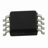
IC SPI FLASH 32MBIT 8SOIC
Manufacturer
Winbond Electronics
Datasheet
1.W25Q32BVZPIG.pdf
(79 pages)
Specifications of W25Q32BVSSIG
Format - Memory
FLASH
Memory Type
FLASH
Memory Size
32M (4M x 8)
Speed
104MHz
Interface
SPI Serial
Voltage - Supply
2.7 V ~ 3.6 V
Operating Temperature
-40°C ~ 85°C
Package / Case
8-SOIC (5.3mm Width), 8-SOP, 8-SOEIAJ
Lead Free Status / RoHS Status
Lead free / RoHS Compliant
Available stocks
Company
Part Number
Manufacturer
Quantity
Price

Company:
Part Number:
W25Q32BVSSIG
Manufacturer:
Winbond
Quantity:
1 000
Company:
Part Number:
W25Q32BVSSIG
Manufacturer:
WINBOND
Quantity:
9 310
Company:
Part Number:
W25Q32BVSSIG
Manufacturer:
Winbond
Quantity:
6 600
Part Number:
W25Q32BVSSIG
Manufacturer:
WINBOND/华邦
Quantity:
20 000


1.
2.
3.
4.
5.
6.
7.
GENERAL DESCRIPTION ............................................................................................................... 5
FEATURES ....................................................................................................................................... 5
PACKAGE TYPES AND PIN CONFIGURATIONS ........................................................................... 6
3.1
3.2
3.3
3.4
3.5
3.6
3.7
3.8
PIN DESCRIPTIONS ...................................................................................................................... 10
4.1
4.2
4.3
4.4
4.5
BLOCK DIAGRAM .......................................................................................................................... 11
FUNCTIONAL DESCRIPTIONS ..................................................................................................... 12
6.1
6.2
STATUS REGISTERS AND INSTRUCTIONS ............................................................................... 14
7.1
Pin Configuration SOIC 208-mil ........................................................................................... 6
Pad Configuration WSON 6x5-mm / 8X6-mm ..................................................................... 6
Pin Configuration PDIP 300-mil ............................................................................................ 7
Pin Description SOIC 208-mil, WSON 6x5/8x6-mm and PDIP 300-mil ............................... 7
Pin Configuration SOIC 300-mil ........................................................................................... 8
Pin Description SOIC 300-mil ............................................................................................... 8
Ball Configuration TFBGA 8x6-mm ...................................................................................... 9
Ball Description TFBGA 8x6-mm ......................................................................................... 9
Chip Select (/CS) ................................................................................................................ 10
Serial Data Input, Output and IOs (DI, DO and IO0, IO1, IO2, IO3) ................................... 10
Write Protect (/WP) ............................................................................................................ 10
HOLD (/HOLD) ................................................................................................................... 10
Serial Clock (CLK) .............................................................................................................. 10
SPI OPERATIONS ............................................................................................................. 12
6.1.1
6.1.2
6.1.3
6.1.4
WRITE PROTECTION ....................................................................................................... 13
6.2.1
STATUS REGISTERS ........................................................................................................ 14
7.1.1
7.1.2
7.1.3
7.1.4
7.1.5
7.1.6
7.1.7
7.1.8
7.1.9
Standard SPI Instructions..................................................................................................... 12
Dual SPI Instructions ............................................................................................................ 12
Quad SPI Instructions .......................................................................................................... 12
Hold Function ....................................................................................................................... 12
Write Protect Features ......................................................................................................... 13
BUSY Status (BUSY) ........................................................................................................... 14
Write Enable Latch Status (WEL) ........................................................................................ 14
Block Protect Bits (BP2, BP1, BP0) ..................................................................................... 14
Top/Bottom Block Protect Bit (TB) ....................................................................................... 14
Sector/Block Protect Bit (SEC) ............................................................................................. 14
Complement Protect Bit (CMP) ............................................................................................ 15
Status Register Protect Bits (SRP1, SRP0) ......................................................................... 15
Erase/Program Suspend Status (SUS) ................................................................................ 15
Security Register Lock Bits (LB3, LB2, LB1) ........................................................................ 15
Table of Contents
- 2 -
W25Q32BV
Related parts for W25Q32BVSSIG
Image
Part Number
Description
Manufacturer
Datasheet
Request
R

Part Number:
Description:
32m-bit Serial Flash Memory With Dual And Quad Spi
Manufacturer:
Winbond Electronics Corp America
Datasheet:
Part Number:
Description:
Winbond H/w Monitoring Ic
Manufacturer:
Winbond Electronics Corp America
Datasheet:
Part Number:
Description:
Winbond Lpc I/o
Manufacturer:
Winbond Electronics Corp America
Datasheet:
Part Number:
Description:
Winbond Smbus Gpi/o
Manufacturer:
Winbond Electronics Corp America
Datasheet:
Part Number:
Description:
Winbond I/o
Manufacturer:
Winbond Electronics Corp America
Datasheet:
Part Number:
Description:
Winbond Clock Generator For Intel P4 Springdale Series Chipset
Manufacturer:
Winbond Electronics Corp America
Datasheet:
Part Number:
Description:
Winbond Clock Generator For Intel P4 Springdale Series Chipset
Manufacturer:
Winbond Electronics Corp America
Datasheet:
Part Number:
Description:
Winbond Clock Generator For Intel P4 Springdale Series Chipset P4 Springdale Series Chipset
Manufacturer:
Winbond Electronics Corp America
Datasheet:
Part Number:
Description:
Winbond Clock Generator For Intel P4 845 Series Chipset
Manufacturer:
Winbond Electronics Corp America
Datasheet:
Part Number:
Description:
Winbond Clock Generator For Via P4/kt Series Chipset
Manufacturer:
Winbond Electronics Corp America
Datasheet:
Part Number:
Description:
Winbond H/w Monitoring Ic
Manufacturer:
Winbond Electronics Corp America
Datasheet:
Part Number:
Description:
Winbond Lpc I/o
Manufacturer:
Winbond Electronics Corp America
Datasheet:
Part Number:
Description:
Winbond Smbus Gpi/o
Manufacturer:
Winbond Electronics Corp America
Datasheet:
Part Number:
Description:
Winbond I/o
Manufacturer:
Winbond Electronics Corp America
Datasheet:

Part Number:
Description:
IC SPI FLASH 4MBIT 8SOIC
Manufacturer:
Winbond Electronics
Datasheet: