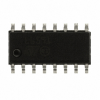
L6591 STMicroelectronics, L6591 Datasheet - Page 5

L6591
Manufacturer Part Number
L6591
Description
IC CTRLR PWM PROG CM HV 16SOIC
Manufacturer
STMicroelectronics
Specifications of L6591
Output Isolation
Isolated
Frequency Range
168 ~ 192kHz
Voltage - Input
8.7 ~ 22 V
Power (watts)
750mW
Operating Temperature
-40°C ~ 150°C
Package / Case
16-SOIC (0.154", 3.90mm Width)
Output Voltage
5 V
Input Voltage
25 V
Operating Temperature Range
- 40 C to + 150 C
Mounting Style
SMD/SMT
Duty Cycle (max)
50 %
For Use With
497-8335 - BOARD EVAL FOR L6591
Lead Free Status / RoHS Status
Lead free / RoHS Compliant
Other names
497-8286
Available stocks
Company
Part Number
Manufacturer
Quantity
Price
Part Number:
L6591
Manufacturer:
ST
Quantity:
20 000
Part Number:
L6591TR
Manufacturer:
ST
Quantity:
20 000
L6591
Table 1.
Pin N.
3
4
5
6
7
8
PFC_STOP
Pin functions (continued)
COMP
Name
VREF
ISEN
OSC
SS
Current sense (PWM comparator) input. The voltage on this pin is internally
compared with an internal reference derived from the voltage on pin COMP
and when they are equal the high-side gate drive output (previously
asserted high by the clock signal generated by the oscillator) is driven low to
turn off the upper power MOSFET; the lower MOSFET is turned on after a
delay programmed by the timing capacitor at pin OSC (#5). The pin is
equipped with 200 ns blanking time for improved noise immunity. A second
comparator referenced at 0.8 V turns off the upper MOSFET if the voltage
at the pin exceeds the threshold, overriding the PWM comparator (pulse-by-
pulse OCP). A third comparison level located at 1.5 V shuts the device
down and brings its consumption almost to a “before start-up” level (hiccup-
mode OCP) to prevent uncontrolled current rise. A logic circuit improves
sensitivity to temporary disturbances.
Soft-start. An internal 20 µA generator charges an external capacitor
connected between the pin and GND (#11) generating a voltage ramp.
During the ramp, the internal reference for pulse-by-pulse OCP (see pin #3,
ISEN) rises linearly starting from zero to its final value, thus causing the
duty cycle of the upper MOSFET to rise starting from zero as well, and all
the functions monitoring pin COMP (#7) are disabled. The same capacitor
is used to delay IC’s shutdown (latch-off or auto-restart mode selectable)
after detecting an overcurrent condition. The SS capacitor is quickly
discharged as the chip goes into UVLO.
Oscillator pin. A resistor to VREF (#6) and a capacitor from the pin to GND
(#11) define the oscillator frequency. The maximum duty cycle is limited
below 50% by an internal T-flip-flop. As a result, the switching frequency will
be half that of the oscillator. The capacitor value defines the dead-time
separating the conduction state of either MOSFET. This capacitor should
not be lower than 220 pF.
Voltage reference. An internal generator furnishes an accurate voltage
reference (5 V±4%, all inclusive) that can be used to supply up to 5 mA to
an external circuit. A small film capacitor (0.1 µF typ.), connected between
this pin and GND (#11) is recommended to ensure the stability of the
generator and to prevent noise from affecting the reference.
Control input for PWM regulation. The pin is to be driven by the
phototransistor (emitter-grounded) of an octocoupler to modulate the
voltage by modulating the current sunk from (sourced by) the pin (0.4 mA
typ.). It is recommended to place a small filter capacitor between the pin
and GND (#11), as close to the IC as possible to reduce switching noise
pick up, to set a pole in the output-to-control transfer function. A voltage
lower than 1.75 V shuts down the IC and reduces its current consumption.
The chip restarts as the voltage exceeds 1.8 V. This function realizes burst-
mode operation at light load.
Open-drain ON/OFF control of PFC controller. This pin is intended for
temporarily stopping the PFC controller at light load in systems comprising
a PFC pre-regulator, during burst-mode operation (see pin COMP, #7). The
pin, normally open, goes low if the voltage on COMP is lower than 1.75 V
and opens when the voltage on pin COMP exceeds 1.8V. Whenever the IC
is shut down (SS > 5 V, DIS > 4.5, ISEN > 1.5 V) the pin is low as well,
provided the supply voltage of the IC is above the restart threshold
(typ. 5 V). It is open during UVLO. Leave the pin open if not used
Doc ID 14821 Rev 5
Function
Pin settings
5/41


