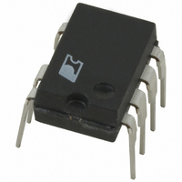
LNK364PN Power Integrations, LNK364PN Datasheet - Page 5

LNK364PN
Manufacturer Part Number
LNK364PN
Description
IC OFFLINE SWIT HV 8DIP
Manufacturer
Power Integrations
Series
LinkSwitch®-XTr
Type
Off Line Switcherr
Datasheet
1.LNK362PG.pdf
(16 pages)
Specifications of LNK364PN
Output Isolation
Isolated
Frequency Range
124 ~ 140kHz
Voltage - Output
700V
Power (watts)
9W
Operating Temperature
-40°C ~ 150°C
Package / Case
8-DIP (0.300", 7.62mm), 7 Leads
Output Voltage
5.8 V
Input / Supply Voltage (max)
265 VAC
Input / Supply Voltage (min)
85 VAC
Duty Cycle (max)
60 %
Switching Frequency
132 KHz
Supply Current
250 uA
Operating Temperature Range
- 40 C to + 150 C
Mounting Style
Through Hole
For Use With
596-1105 - DESIGN ACCELERATOR KIT XT SWITCH
Lead Free Status / RoHS Status
Lead free / RoHS Compliant
Other names
596-1088-2
596-1088-2
596-1088-5
596-1088-2
596-1088-5
Available stocks
Company
Part Number
Manufacturer
Quantity
Price
Company:
Part Number:
LNK364PN
Manufacturer:
PowerInt
Quantity:
2 300
Part Number:
LNK364PN
Manufacturer:
POWER
Quantity:
20 000
The LinkSwitch-XT is completely self-powered from the DRAIN
pin, requiring only a small ceramic capacitor C3 connected to
the BYPASS pin. No auxiliary winding on the transformer is
required.
Key Application Considerations
LinkSwitch-XT Design Considerations
Output Power Table
The data sheet maximum output power table (Table 1) represents
the maximum practical continuous output power level that can
be obtained under the following assumed conditions:
1. The minimum DC input voltage is 90 V or higher for 85 VAC
2. Secondary output of 6 V with a fast PN rectifi er diode.
3. Assumed effi ciency of 70%.
4. Voltage only output (no secondary-side constant current
5. Discontinuous mode operation (K
6. A primary clamp (RCD or Zener) is used.
7. The part is board mounted with SOURCE pins soldered
8. Ambient temperature of 50 °C for open frame designs
Below a value of 1, K
current. Above a value of 1, K
OFF time to the secondary diode conduction time. Due to
the fl ux density requirements described below, typically a
LinkSwitch-XT design will be discontinuous, which also has
the benefi ts of allowing lower cost fast (instead of ultra-fast)
output diodes and reducing EMI.
Clampless Designs
Clampless designs rely solely on the drain node capacitance
to limit the leakage inductance induced peak drain-to-source
voltage. Therefore, the maximum AC input line voltage, the
value of V
leakage inductance and peak primary current, and the primary
winding capacitance determine the peak drain voltage. With no
signifi cant dissipative element present, as is the case with an
external clamp, the longer duration of the leakage inductance
ringing can increase EMI.
The following requirements are recommended for a universal
input or 230 VAC only Clampless design:
1. A Clampless design should only be used for P
input, or 240 V or higher for 230 VAC input or 115 VAC
with a voltage doubler. The value of the input capacitance
should be large enough to meet these criteria for AC input
designs.
circuit).
to a suffi cient area of copper to keep the SOURCE pin
temperature at or below 100 °C.
and an internal enclosure temperature of 60 °C for adapter
designs.
using the LNK362
OR
, the leakage inductance energy, a function of
†
P
and a V
is the ratio of ripple to peak primary
P
is the ratio of primary MOSFET
OR
** ≤ 90 V.
P
>1).
O
≤ 2.5 W,
2. For designs where P
3. For designs where 2 < P
4. For designs where P
5. Ensure that worst-case high line, peak drain voltage is below
†For 110 VAC only input designs it may be possible to extend
the power range of Clampless designs to include the LNK363.
However, the increased leakage ringing may degrade EMI
performance.
**V
drop that is refl ected to the primary via the turns ratio of the
transformer during the diode conduction time. The V
to the DC bus voltage and the leakage spike to determine the
peak drain voltage.
Audible Noise
The cycle skipping mode of operation used in LinkSwitch-XT
can generate audio frequency components in the transformer.
To limit this audible noise generation, the transformer should
be designed such that the peak core fl ux density is below
1500 Gauss (150 mT). Following this guideline and using the
standard transformer production technique of dip varnishing
practically eliminates audible noise. Vacuum impregnation
of the transformer should not be used due to the high primary
capacitance and increased losses that result. Higher fl ux densities
are possible, however careful evaluation of the audible noise
performance should be made using production transformer
samples before approving the design.
Ceramic capacitors that use dielectrics, such as Z5U, when
used in clamp circuits may also generate audio noise. If this is
the case, try replacing them with a capacitor having a different
dielectric or construction, for example a fi lm type.
LinkSwitch-XT Layout Considerations
See Figure 6 for a recommended circuit board layout for
LinkSwitch-XT (P & G package).
Single Point Grounding
Use a single point ground connection from the input fi lter capacitor
to the area of copper connected to the SOURCE pins.
used to ensure adequate primary intra-winding capacitance
in the range of 25 pF to 50 pF.
added to the transformer using a standard recovery rectifi er
diode to act as a clamp. This bias winding may also be used
to externally power the device by connecting a resistor from
the bias-winding capacitor to the BYPASS pin. This inhibits
the internal high-voltage current source, reducing device
dissipation and no-load consumption.
practical and an external RCD or Zener clamp should be
used.
the BV
≤ 650 V to allow margin for design variation.
OR
is the secondary output plus output diode forward voltage
DSS
specifi cation of the internal MOSFET and ideally
O
O
≤ 2 W, a two-layer primary should be
> 2.5 W Clampless designs are not
O
≤ 2.5 W, a bias winding should be
LNK362-364
OR
Rev. E 11/08
2-5
adds
5


