TOP234GN Power Integrations, TOP234GN Datasheet - Page 4
TOP234GN
Manufacturer Part Number
TOP234GN
Description
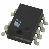
IC OFFLINE SWIT OVP UVLO 8SMD
Manufacturer
Power Integrations
Series
TOPSwitch®-FXr
Type
Off Line Switcherr
Datasheet
1.TOP234YN.pdf
(36 pages)
Specifications of TOP234GN
Output Isolation
Isolated
Frequency Range
66 ~ 132kHz
Voltage - Output
700V
Power (watts)
30W
Operating Temperature
-40°C ~ 150°C
Package / Case
8-SMD Gull Wing, 7 Leads
Output Voltage
12 V
Input / Supply Voltage (max)
265 VAC
Input / Supply Voltage (min)
85 VAC
Duty Cycle (max)
78 %
Switching Frequency
132 KHz
Supply Current
1.5 mA
Operating Temperature Range
- 40 C to + 150 C
Mounting Style
SMD/SMT
Lead Free Status / RoHS Status
Lead free / RoHS Compliant
Available stocks
Company
Part Number
Manufacturer
Quantity
Price
Company:

Part Number:
TOP234GN
Manufacturer:
PowerInt
Quantity:
350
Part Number:
TOP234GN
Manufacturer:
POWER
Quantity:
20 000
Part Number:
TOP234GN-TL
Manufacturer:
POWER
Quantity:
20 000


TOPSwitch-FX Family Functional Description
Like TOPSwitch, TOPSwitch-FX is an integrated switched
mode power supply chip that converts a current at the control
input to a duty cycle at the open drain output of a high voltage
power MOSFET. During normal operation the duty cycle of the
power MOSFET decreases linearly with increasing CONTROL
pin current as shown in Figure 4.
In addition to the three terminal TOPSwitch features, such as the
high voltage start-up, the cycle-by-cycle current limiting, loop
compensation circuitry, auto-restart, thermal shutdown, etc.,
the TOPSwitch-FX incorporates many additional functions that
reduce system cost, increase power supply performance and
design flexibility. A patented high voltage CMOS technology
allows both the high voltage power MOSFET and all the low
voltage control circuitry to be cost effectively integrated onto a
single monolithic chip.
Two terminals, FREQUENCY (available only in Y package)
and MULTI-FUNCTION, have been added to implement some
of the new functions. These terminals can be connected to the
SOURCE pin to operate the TOPSwitch-FX in a TOPSwitch-
like three terminal mode. However, even in this three terminal
mode, the TOPSwitch-FX offers many new transparent features
that do not require any external components:
1. A fully integrated 10 ms soft-start reduces peak currents and
2. DC
3. Cycle skipping at minimum pulse width achieves regulation
4. Higher switching frequency of 132 kHz reduces the
5. Frequency jittering reduces EMI.
6. Hysteretic over-temperature shutdown ensures automatic
7. Packages with omitted pins and lead forming provide large
8. Tighter absolute tolerances and smaller temperature vari-
The MULTI-FUNCTION pin is usually used for line sensing by
connecting a resistor from this pin to the rectified DC high
voltage bus to implement line over-voltage (OV)/under-voltage
(UV) and line feed forward with DC
mode, the value of the resistor determines the OV/UV thresholds
and the DC
above the under-voltage threshold. In high efficiency
applications, this pin can be used in the external current limit
mode instead, to reduce the current limit externally (to a value
4
TOP232-234
voltages during start-up and practically eliminates output
overshoot in most applications.
input voltage requirement and/or higher power capability.
and very low power consumption at no load.
transformer size with no noticeable impact on EMI or on
high line efficiency.
recovery from thermal fault. Large hysteresis prevents circuit
board overheating.
DRAIN creepage distance.
ations on switching frequency, current limit and PWM gain.
MAX
B
7/01
of 78% allows smaller input storage capacitor, lower
MAX
is reduced linearly starting from a line voltage
MAX
reduction. In this
Figure 4. Relationship of Duty Cycle to CONTROL Pin Current.
close to the operating peak current), by connecting the pin to
SOURCE through a resistor. The same pin can also be used as
a remote ON/OFF and a synchronization input in both modes.
The FREQUENCY pin in the TO-220 package sets the switching
frequency to the default value of 132 kHz when connected to
SOURCE pin. A half frequency option can be chosen by
connecting this pin to CONTROL pin instead. Leaving this pin
open is not recommended.
CONTROL (C) Pin Operation
The CONTROL pin is a low impedance node that is capable of
receiving a combined supply and feedback current. During
normal operation, a shunt regulator is used to separate the
feedback signal from the supply current. CONTROL pin voltage
V
MOSFET gate driver. An external bypass capacitor closely
connected between the CONTROL and SOURCE pins is
required to supply the instantaneous gate drive current. The
total amount of capacitance connected to this pin also sets the
auto-restart timing as well as control loop compensation.
When rectified DC high voltage is applied to the DRAIN pin
during start-up, the MOSFET is initially off, and the CONTROL
pin capacitor is charged through a switched high voltage current
source connected internally between the DRAIN and CONTROL
pins. When the CONTROL pin voltage V
approximately 5.8 V, the control circuitry is activated and the
soft-start begins. The soft-start circuit gradually increases the
duty cycle of the MOSFET from zero to the maximum value
over approximately 10 ms. If no external feedback/supply
current is fed into the CONTROL pin by the end of the soft-start,
the high voltage current source is turned off and the CONTROL
pin will start discharging in response to the supply current
drawn by the control circuitry. If the power supply is designed
properly, and no fault condition such as open loop or shorted
output exists, the feedback loop will close, providing external
C
is the supply voltage for the control circuitry including the
78
47
1.5
Auto-restart
I
CD1
1.5
1.9
I
M
= 190 µA
I
B
I
C
(mA)
Slope = PWM Gain
I
M
= 140 µA
I
PI-2504-072799
M
5.5 5.9
C
< I
M(DC)
reaches
Related parts for TOP234GN
Image
Part Number
Description
Manufacturer
Datasheet
Request
R

Part Number:
Description:
SOP-16
Manufacturer:
Power Integrations
Datasheet:
Part Number:
Description:
DIP8
Manufacturer:
Power Integrations
Datasheet:
Part Number:
Description:
TO-263
Manufacturer:
Power Integrations
Datasheet:
Part Number:
Description:
TO-263
Manufacturer:
Power Integrations
Datasheet:
Part Number:
Description:
Manufacturer:
Power Integrations
Datasheet: