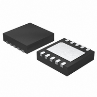
LTC3202EDD Linear Technology, LTC3202EDD Datasheet - Page 10

LTC3202EDD
Manufacturer Part Number
LTC3202EDD
Description
IC LED DRIVR WHITE BCKLGT 10-DFN
Manufacturer
Linear Technology
Type
Backlight, White LEDr
Datasheet
1.LTC3202EDDPBF.pdf
(12 pages)
Specifications of LTC3202EDD
Topology
PWM, Switched Capacitor (Charge Pump)
Number Of Outputs
1
Internal Driver
Yes
Type - Primary
Backlight
Type - Secondary
White LED
Frequency
1.5MHz
Voltage - Supply
2.7 V ~ 4.5 V
Mounting Type
Surface Mount
Package / Case
10-DFN
Operating Temperature
-40°C ~ 85°C
Current - Output / Channel
125mA
Internal Switch(s)
Yes
Lead Free Status / RoHS Status
Contains lead / RoHS non-compliant
Voltage - Output
-
Efficiency
-
Available stocks
Company
Part Number
Manufacturer
Quantity
Price
Company:
Part Number:
LTC3202EDD
Manufacturer:
LT
Quantity:
10 000
Part Number:
LTC3202EDD#PBF
Manufacturer:
LINEAR/凌特
Quantity:
20 000
Company:
Part Number:
LTC3202EDD#TR
Manufacturer:
LT
Quantity:
1 200
Company:
Part Number:
LTC3202EDD#TRPBF
Manufacturer:
LT
Quantity:
5 123
LTC3202
OPERATIO
Layout Considerations
Due to its high switching frequency and the transient
currents produced by the LTC3202, careful board layout is
necessary. A true ground plane and short connections to
all capacitors will improve performance and ensure proper
regulation under all conditions. Figure 6 shows the recom-
mended layout configurations.
The flying capacitor pins C1
very high edge rate waveforms. The large dv/dt on these
pins can couple energy capacitively to adjacent printed
circuit board runs. Magnetic fields can also be generated
if the flying capacitors are not close to the LTC3202 (i.e.
the loop area is large). To decouple capacitive energy
transfer, a Faraday shield may be used. This is a grounded
PC trace between the sensitive node and the LTC3202
pins. For a high quality AC ground it should be returned to
a solid ground plane that extends all the way to the
LTC3202.
10
V
OUT
V
GND
OUT
V
IN
V
IN
Figure 6. Recommended Layouts
U
D1
GND
+
, C2
+
, C1
D0
–
and C2
–
3202 F06
will have
Thermal Management
For higher input voltages and maximum output current
there can be substantial power dissipation in the LTC3202.
If the junction temperature increases above approxi-
mately 160 C the thermal shutdown circuitry will auto-
matically deactivate the output. To reduce the maximum
junction temperature, a good thermal connection to the
PC board is recommended. Connecting the GND pin (Pin
5 and Pin 11 on the DFN package) to a ground plane, and
maintaining a solid ground plane under the device can
reduce the thermal resistance of the package and PC
board considerably.
Brightness Control Using Pulse Width Modulation
An alternative approach to dimming is to use pulse width
modulation rather than the internal digital to analog con-
verter. By connecting both the D0 and D1 pins to a PWM
signal, continuous brightness control can be achieved.
Frequencies from 100Hz to 500Hz are acceptable with a
1 F to 4.7 F output capacitor.
V
D0, D1
Figure 7. Alternative Brightness Control
t
10
1
D0
D1
LTC3202
3202 F07
3202fa


