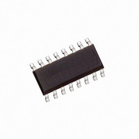
HCPL-316J Avago Technologies US Inc., HCPL-316J Datasheet - Page 29

HCPL-316J
Manufacturer Part Number
HCPL-316J
Description
OPTOCOUPLER GATE DRV 2A 16-SOIC
Manufacturer
Avago Technologies US Inc.
Datasheet
1.HCPL-316J-500E.pdf
(33 pages)
Specifications of HCPL-316J
Configuration
High-Side
Input Type
Differential
Delay Time
300ns
Current - Peak
2.5A
Number Of Configurations
1
Number Of Outputs
1
Voltage - Supply
4.5 V ~ 5.5 V
Operating Temperature
-40°C ~ 100°C
Mounting Type
Surface Mount
Package / Case
16-SOIC (0.300", 7.5mm Width)
No. Of Channels
1
Isolation Voltage
3.75kV
Optocoupler Output Type
Gate Drive
Input Current
22mA
Output Voltage
30V
Opto Case Style
SOIC
No. Of Pins
16
Propagation Delay Low-high
0.5µs
Lead Free Status / RoHS Status
Contains lead / RoHS non-compliant
High Side Voltage - Max (bootstrap)
-
Lead Free Status / RoHS Status
Contains lead / RoHS non-compliant, Contains lead / RoHS non-compliant
Other names
516-1130-5
Available stocks
Company
Part Number
Manufacturer
Quantity
Price
Company:
Part Number:
HCPL-316J
Manufacturer:
AVAGO
Quantity:
20 700
Company:
Part Number:
HCPL-316J
Manufacturer:
AD
Quantity:
1 939
Part Number:
HCPL-316J
Manufacturer:
AGILENT
Quantity:
20 000
Company:
Part Number:
HCPL-316J#500
Manufacturer:
AGILENT
Quantity:
3 169
Part Number:
HCPL-316J#500
Manufacturer:
AGILENT
Quantity:
20 000
Company:
Part Number:
HCPL-316J-000E
Manufacturer:
KOITECH
Quantity:
713
Company:
Part Number:
HCPL-316J-000E
Manufacturer:
AVAGO
Quantity:
21 000
Part Number:
HCPL-316J-000E
Manufacturer:
AVAGO/安华高
Quantity:
20 000
Part Number:
HCPL-316J-500E
Manufacturer:
AVAGO/安华高
Quantity:
20 000
Part Number:
HCPL-316J-500E/HCPL316J-500E
Manufacturer:
AVAGO/安华高
Quantity:
20 000
HCPL-316J
Higher Output Current Using an External Current Buf-
fer:
To increase the IGBT gate drive current, a non-inverting
current buffer (such as the npn/pnp buffer shown in
Figure 75) may be used. Inverting types are not com-
patible with the desatura-tion fault protection circuitry
and should be avoided. To preserve the slow IGBT turn-
off feature during a fault condition, a 10 nF capacitor
should be connected from the buffer input to V
a 10 : resistor inserted between the output and the
common npn/pnp base. The MJD44H11/MJD45H11
pair is appropriate for currents up to 8A maximum. The
D44VH10/ D45VH10 pair is appropriate for currents up
to 15 A maximum.
Figure 75. Current buffer for increased drive current.
Part Number
MUR1100E
MURS160T3
UF4007
BYM26E
BYV26E
BYV99
Power/Layout Considerations
Operating Within the Maximum Allowable Power Ratings
(Adjusting Value of R
When choosing the value of R
firm that the power dissipation of the HCPL-316J is
within the maximum allowable power rating.
The steps for doing this are:
1. Calculate the minimum desired R
29
V
DESAT
LED2+
V
V
OUT
V
V
CC2
V
V
EE
EE
E
C
16
15
14
13
12
11
10
9
10 Ω
G
10 nF
100 pF
):
Manufacturer
Motorola
Motorola
General Semi.
Philips
Philips
Philips
15 V
G
-5 V
, it is important to con-
MJD44H11 or
MJD45H11 or
G
4.5 Ω
2.5 Ω
;
D44VH10
D45VH10
t
75
75
75
75
75
75
rr
(ns)
EE
and
Max. Reverse Voltage
Rating, V
1000
600
1000
1000
1000
600
2. Calculate total power dissipation in the part referring
3. Compare the input and output power dissipation
DESAT Diode and DESAT Threshold
The DESAT diode’s function is to conduct forward cur-
rent, allowing sensing of the IGBT’s saturated collector-
to-emitter voltage, V
block high voltages (when the IGBT is “off”). During the
short period of time when the IGBT is switching, there is
commonly a very high dV
the IGBT’s collector-to-emitter. This results in I
C
the blanking capacitor, C
this charging current and avoid false DESAT triggering,
it is best to use fast response diodes. Listed in the be-
low table are fast-recovery diodes that are suitable for
use as a DESAT diode (D
plication circuit shown in Figure 62, the voltage on pin
14 (DESAT) is V
ON voltage of D
emitter voltage). The value of V
to signal a FAULT condition, is nominally 7V – V
sired, this DESAT threshold voltage can be decreased by
using multiple DESAT diodes in series. If n is the number
of DESAT diodes then the nominal threshold value be-
comes V
diodes instead of one, diodes with half of the total re-
quired maximum reverse-voltage rating may be chosen.
D-DESAT
to Figure 77. (Average switching energy supplied to
HCPL-316J per cycle vs. R
calculated in step #2 to the maximum recommended
dissipation for the HCPL-316J. (If the maximum rec-
ommended level has been exceeded, it may be nec-
essary to raise the value of R
power and repeat step #2.)
RRM
(Volts)
CE,FAULT(TH)
x dV
CE
DESAT
/dt) charging current which will charge
DESAT
= 7 V – n x V
CESAT
= V
and V
DESAT
F
59-04 (axial leaded)
Case 403A (surface mount)
DO-204AL (axial leaded)
SOD64 (axial leaded)
SOD57 (axial leaded)
SOD87 (surface mount)
, (when the IGBT is “on”) and to
+ V
CE
G
BLANK
/dt voltage ramp rate across
plot);
CE
CE
Package Type
). In the recommended ap-
, (where V
F
G
is the IGBT collector-to-
CE
. In the case of using two
. In order to minimize
to lower the switching
which triggers DESAT
F
is the forward
CHARGE
F
. If de-
(=


