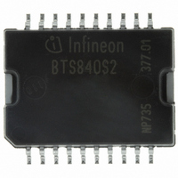
BTS840S2 Infineon Technologies, BTS840S2 Datasheet

BTS840S2
Specifications of BTS840S2
BTS840S2INTR
BTS840S2NT
BTS840S2T
SP000011324
Available stocks
Related parts for BTS840S2
BTS840S2 Summary of contents
Page 1
... Loss of ground and loss of V Electrostatic discharge protection (ESD) Diagnostic Functions Proportinal load current sense Diagnostic feedback with open drain output Open load detection in OFF-state with external resistor Feedback of thermal shutdown in ON-state Infineon technologies 5.0...34V bb(on) two parallel 30m 15m ON ...
Page 2
... IS1 Sense current output 1,2; proportional to the load current, zero in the case of current 9 IS2 limitation of the load current Heatslug V bb Positiv powersupply voltage. Good way to design a very low thermal resistance. Infineon technologies gate current limit control + charge clamp for logic pump ...
Page 3
... set up without the DUT connected to the generator per ISO 7637-1 and DIN 40839 Load dump ) 4 Device on 50mm*50mm*1.5mm epoxy PCB FR4 with 6cm connection. PCB is vertical without blown air. Infineon technologies = 25°C unless otherwise specified 13 ...
Page 4
... L Slew rate 30 OUT L Slew rate off 40 OUT not subject to production test, specified by design ) 6 See timing diagram on page 11. Infineon technologies Symbol each channel: R thjs one channel active: R thja all channels active: Symbol each of the two channels 25° 150° 25° ON(NL =-40...+150° ...
Page 5
... Integrated protection functions are designed to prevent IC destruction under fault conditions described in the 11 data sheet. Fault conditions are considered as "outside" normal operating range. Protection functions are not designed for continuous repetitive operation. Infineon technologies Symbol each of the two channels V bb(on) V bb(under) T =-40...+25° ...
Page 6
... In the case of current limitation the sense current I High. See figure 2c, page 12. 15) V Valid if was exceeded before. bb(u rst) 16) not subject to production test, specified by design Infineon technologies Symbol each of the two channels 12) =-40° =25°C...150°C: T ...
Page 7
... Status leakage current 17) not subject to production test, specified by design 18) External pull up resistor required for open load detection in off state. 19) If ground resistors R are used, add the voltage drop across these resistors. GND Infineon technologies Symbol each of the two channels static after soff(IS ...
Page 8
... An external short of output used, an offset voltage at the GND and ST pins will occur and the V ) Low ohmic short may reduce the output current bb ) Power Transistor off, high impedance 23 ) with external resistor between V 24 Infineon technologies Current Status 1 Sense 1 Current Status 2 Sense 2 level level ...
Page 9
... The use of ESD zener diodes as voltage clamp at DC conditions is not recommended. Current sense output, IS1 or IS2 I IS ESD-ZD GND ESD-Zener diode: 6.1 V typ., max 14 mA nominal IS Infineon technologies Inductive and overvoltage output clamp, IN1 or IN2 OUT1 or OUT2 clamped +5V Overvoltage and reverse batt. Protection ST For each channel ...
Page 10
... Consider at your PCB layout that in the case of Vbb dis- connection with energized inductive load all the load current flows through the GND connection. Infineon technologies Inductive load switch-off energy dissipation OUT = ...
Page 11
... The sense signal is not valid during settling time after turn or change of load current. Figure 1b: V turn on: bb IN1 IN2 OUT1 V OUT2 ST1 open drain ST2 open drain proper turn on under all conditions Infineon technologies Figure 2a: Switching a resistive load, turn-on/off time and slew rate definition OUT doff(ST) 90% t off t slc(IS) 10 ...
Page 12
... Figure 2d: Switching an inductive load OUT L(OL the time constant of load is too large, open-load-status may occur Infineon technologies Figure 3a: Turn on into short circuit: shut down by overtemperature, restart by cooling IN1 other channel: normal operation L(lim) t off(SC Heating up of the chip may require several milliseconds, depending ...
Page 13
... Figure 4a: Overtemperature: Reset if T < Figure 5a: Open load: detection (with R turn on/off to open load OUT I L open load I IS Infineon technologies Figure 6a: Undervoltage Figure 6b: Undervoltage restart of charge pump ), EXT d(ST OL3) off- state V bb(u rst) V bb(under) t charge pump starts BTS 840 S2 not defined ...
Page 14
... This range for the current sense ratio refers to all devices. The accuracy of the k least by a factor of two by matching the value of k for every single device. ILIS Infineon technologies Figure 8b: Current sense ratio: 15000 V bb(o rst) 10000 5000 Figure 9a: Output voltage drop versus load current: ...
Page 15
... Infineon Technologies is an approved CECC manufacturer. Information For further information on technology, delivery terms and conditions and prices please contact your nearest Infineon Technologies Office in Germany or our Infineon Technologies Representatives worldwide (see address list). Warnings Due to technical requirements components may contain dangerous substances ...


