VND5N07 STMicroelectronics, VND5N07 Datasheet - Page 4
VND5N07
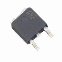
Manufacturer Part Number
VND5N07
Description
MOSFET N-CH 70V 5A DPAK
Manufacturer
STMicroelectronics
Series
OMNIFET II™r
Type
Low Sider
Datasheet
1.VND5N0713TR.pdf
(24 pages)
Specifications of VND5N07
Input Type
Non-Inverting
Number Of Outputs
1
On-state Resistance
200 mOhm
Current - Peak Output
5A
Mounting Type
Surface Mount
Package / Case
DPak, TO-252 (2 leads+tab), SC-63
Transistor Polarity
N-Channel
Resistance Drain-source Rds (on)
0.2 Ohms
Forward Transconductance Gfs (max / Min)
4 S
Drain-source Breakdown Voltage
70 V
Continuous Drain Current
5 A
Power Dissipation
60000 mW
Maximum Operating Temperature
+ 150 C
Mounting Style
SMD/SMT
Minimum Operating Temperature
- 40 C
Lead Free Status / RoHS Status
Lead free / RoHS Compliant
Voltage - Supply
-
Operating Temperature
-
Current - Output / Channel
-
Lead Free Status / Rohs Status
Lead free / RoHS Compliant
Other names
497-2481-5
497-3302-5
497-3302-5
VND5N07-E
497-3302-5
497-3302-5
VND5N07-E
Available stocks
Company
Part Number
Manufacturer
Quantity
Price

Company:
Part Number:
VND5N07-1
Manufacturer:
ST
Quantity:
12 500
Company:
Part Number:
VND5N07-13TR
Manufacturer:
ST
Quantity:
1 831
Company:
Part Number:
VND5N07FI
Manufacturer:
ST
Quantity:
12 500
Company:
Part Number:
VND5N07TR-E
Manufacturer:
INF
Quantity:
6 392
Part Number:
VND5N07TR-E
Manufacturer:
ST
Quantity:
20 000


List of figures
List of figures
Figure 1.
Figure 2.
Figure 3.
Figure 4.
Figure 5.
Figure 6.
Figure 7.
Figure 8.
Figure 9.
Figure 10.
Figure 11.
Figure 12.
Figure 13.
Figure 14.
Figure 15.
Figure 16.
Figure 17.
Figure 18.
Figure 19.
Figure 20.
Figure 21.
Figure 22.
Figure 23.
Figure 24.
Figure 25.
Figure 26.
Figure 27.
Figure 28.
Figure 29.
Figure 30.
Figure 31.
Figure 32.
Figure 33.
4/24
Block diagram . . . . . . . . . . . . . . . . . . . . . . . . . . . . . . . . . . . . . . . . . . . . . . . . . . . . . . . . . . . . 5
Switching time test circuit for resistive load . . . . . . . . . . . . . . . . . . . . . . . . . . . . . . . . . . . . . 9
Test circuit for diode recovery times . . . . . . . . . . . . . . . . . . . . . . . . . . . . . . . . . . . . . . . . . . . 9
Unclamped inductive load test circuits . . . . . . . . . . . . . . . . . . . . . . . . . . . . . . . . . . . . . . . . 10
Input charge test circuit. . . . . . . . . . . . . . . . . . . . . . . . . . . . . . . . . . . . . . . . . . . . . . . . . . . . 10
Unclamped inductive waveforms . . . . . . . . . . . . . . . . . . . . . . . . . . . . . . . . . . . . . . . . . . . . 11
Switching waveforms . . . . . . . . . . . . . . . . . . . . . . . . . . . . . . . . . . . . . . . . . . . . . . . . . . . . . 11
Thermal impedance for ISOWATT220 . . . . . . . . . . . . . . . . . . . . . . . . . . . . . . . . . . . . . . . . 12
Thermal impedance for DPAK / IPAK . . . . . . . . . . . . . . . . . . . . . . . . . . . . . . . . . . . . . . . . . 12
Source-Drain diode forward characteristics . . . . . . . . . . . . . . . . . . . . . . . . . . . . . . . . . . . . 13
Static Drain-Source on resistance . . . . . . . . . . . . . . . . . . . . . . . . . . . . . . . . . . . . . . . . . . . 13
Derating curve . . . . . . . . . . . . . . . . . . . . . . . . . . . . . . . . . . . . . . . . . . . . . . . . . . . . . . . . . . 13
Static Drain-Source on resistance vs. input voltage . . . . . . . . . . . . . . . . . . . . . . . . . . . . . . 13
Normalized on resistance Vs temperature . . . . . . . . . . . . . . . . . . . . . . . . . . . . . . . . . . . . . 13
Transconductance . . . . . . . . . . . . . . . . . . . . . . . . . . . . . . . . . . . . . . . . . . . . . . . . . . . . . . . 13
Static Drain-Source on resistance Vs. Id . . . . . . . . . . . . . . . . . . . . . . . . . . . . . . . . . . . . . . 14
Switching time resistive load. . . . . . . . . . . . . . . . . . . . . . . . . . . . . . . . . . . . . . . . . . . . . . . . 14
Turn-on current slope . . . . . . . . . . . . . . . . . . . . . . . . . . . . . . . . . . . . . . . . . . . . . . . . . . . . . 14
Turn-on current slope . . . . . . . . . . . . . . . . . . . . . . . . . . . . . . . . . . . . . . . . . . . . . . . . . . . . . 14
Input voltage Vs. input charge . . . . . . . . . . . . . . . . . . . . . . . . . . . . . . . . . . . . . . . . . . . . . . 14
Turn-off Drain source voltage slope . . . . . . . . . . . . . . . . . . . . . . . . . . . . . . . . . . . . . . . . . . 14
Turn-off Drain-Source voltage slope . . . . . . . . . . . . . . . . . . . . . . . . . . . . . . . . . . . . . . . . . . 15
Capacitance variations . . . . . . . . . . . . . . . . . . . . . . . . . . . . . . . . . . . . . . . . . . . . . . . . . . . . 15
Switching time resistive load. . . . . . . . . . . . . . . . . . . . . . . . . . . . . . . . . . . . . . . . . . . . . . . . 15
Step response current limit . . . . . . . . . . . . . . . . . . . . . . . . . . . . . . . . . . . . . . . . . . . . . . . . . 15
Output characteristics . . . . . . . . . . . . . . . . . . . . . . . . . . . . . . . . . . . . . . . . . . . . . . . . . . . . . 15
Normalized on resistance Vs. temperature. . . . . . . . . . . . . . . . . . . . . . . . . . . . . . . . . . . . . 15
Normalized Input threshold voltage Vs. temperature . . . . . . . . . . . . . . . . . . . . . . . . . . . . . 16
Normalized current limit Vs. junction temperature . . . . . . . . . . . . . . . . . . . . . . . . . . . . . . . 16
DPAK package dimensions . . . . . . . . . . . . . . . . . . . . . . . . . . . . . . . . . . . . . . . . . . . . . . . . 18
IPAK mechanical data and package outline . . . . . . . . . . . . . . . . . . . . . . . . . . . . . . . . . . . . 20
ISOWATT220 mechanical data and package outline . . . . . . . . . . . . . . . . . . . . . . . . . . . . . 21
SOT-82FM mechanical data and package outline . . . . . . . . . . . . . . . . . . . . . . . . . . . . . . . 22
VND5N07
Related parts for VND5N07
Image
Part Number
Description
Manufacturer
Datasheet
Request
R

Part Number:
Description:
STMicroelectronics [RIPPLE-CARRY BINARY COUNTER/DIVIDERS]
Manufacturer:
STMicroelectronics
Datasheet:
Part Number:
Description:
STMicroelectronics [LIQUID-CRYSTAL DISPLAY DRIVERS]
Manufacturer:
STMicroelectronics
Datasheet:

Part Number:
Description:
BOARD EVAL FOR MEMS SENSORS
Manufacturer:
STMicroelectronics
Datasheet:
Part Number:
Description:
NPN TRANSISTOR POWER MODULE
Manufacturer:
STMicroelectronics
Datasheet:
Part Number:
Description:
TURBOSWITCH ULTRA-FAST HIGH VOLTAGE DIODE
Manufacturer:
STMicroelectronics
Datasheet:
Part Number:
Description:
Manufacturer:
STMicroelectronics
Datasheet:
Part Number:
Description:
DIODE / SCR MODULE
Manufacturer:
STMicroelectronics
Datasheet:
Part Number:
Description:
DIODE / SCR MODULE
Manufacturer:
STMicroelectronics
Datasheet:
Part Number:
Description:
Search -----> STE16N100
Manufacturer:
STMicroelectronics
Datasheet:
Part Number:
Description:
Search ---> STE53NA50
Manufacturer:
STMicroelectronics
Datasheet:
Part Number:
Description:
NPN Transistor Power Module
Manufacturer:
STMicroelectronics
Datasheet:
Part Number:
Description:
DIODE / SCR MODULE
Manufacturer:
STMicroelectronics
Datasheet: