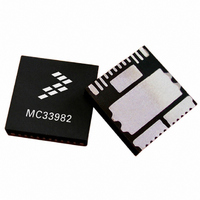
MC33982BPNA Freescale Semiconductor, MC33982BPNA Datasheet - Page 22

MC33982BPNA
Manufacturer Part Number
MC33982BPNA
Description
IC SWITCH HI SIDE SINGLE 16-PQFN
Manufacturer
Freescale Semiconductor
Type
High Sider
Datasheet
1.MC33982BPNA.pdf
(36 pages)
Specifications of MC33982BPNA
Input Type
SPI
Number Of Outputs
1
On-state Resistance
2 mOhm
Voltage - Supply
6 V ~ 27 V
Operating Temperature
-40°C ~ 125°C
Mounting Type
Surface Mount
Package / Case
16-PQFN, 16-PowerQFN
Lead Free Status / RoHS Status
Contains lead / RoHS non-compliant
Current - Output / Channel
-
Current - Peak Output
-
Available stocks
Company
Part Number
Manufacturer
Quantity
Price
Part Number:
MC33982BPNA
Manufacturer:
FREESCALE
Quantity:
20 000
SPI PROTOCOL DESCRIPTION
synchronous data transfer with four I /O lines associated with
it: Serial Clock (SCLK), Serial Input (SI), Serial Output (SO),
and Chip Select (
most significant bit (MSB) first. All inputs are compatible with
5.0 V CMOS logic levels.
SERIAL CLOCK (SCLK)
33982 device. The serial input pin (SI) accepts data into the
input shift register on the falling edge of the SCLK signal
while the serial output pin (SO) shifts data information out of
the SO line driver on the rising edge of the SCLK signal. It is
important that the SCLK pin be in a logic LOW state
whenever
recommended that the SCLK pin be in a Logic [0] state
whenever the device is not accessed (
SCLK has an active internal pull-down, I
Logic [1], signals at the SCLK and SI pins are ignored and SO
is tri-stated (high-impedance). (See
Figure
SERIAL INTERFACE (SI)
instruction is read on the falling edge of SCLK. An 8-bit
22
D0) protocol with both input and output words transferring the
33982
FUNCTIONAL DEVICE OPERATION
LOGIC COMMANDS AND REGISTERS
The SPI interface has a full duplex, three-wire
The SI / SO pins of the 33982 follow a first-in first-out (D7 /
The SPI lines perform the following functions:
The SCLK pin clocks the internal shift registers of the
This is a serial interface (SI) command data input pin. SI
11.)
CS
makes any transition. For this reason, it is
CS
).
NOTES:
Notes
1.
2.
3.
1. RST is a Logic [1] state during the above operation.
2. D7:D0 relate to the most recent ordered entry of data into the device.
3. OD7:OD0 relate to the first 8 bits of ordered fault and status data out of the device.
CSB
SCLK
CS
SO
SO
SI
RSTB is in a logic 1 state during the above operation.
D0, D1, D2, ..., and D7 relate to the most recent ordered entry of data into the SPSS
OD0, OD1, OD2, ..., and OD7 relate to the first 8 bits of ordered fault and status data out
of the device.
RST
Figure 10
Figure 10. Single 8-Bit Word SPI Communication
FUNCTIONAL DEVICE OPERATION
CS
DWN
LOGIC COMMANDS AND REGISTERS
Logic [1] state).
D7
OD7
. When
and
D6
OD6
CS
D5
is
OD5
D4
OD4
stream of serial data is required on the SI pin, starting with D7
to D0. The internal registers of the 33982 are configured and
controlled using a 4-bit addressing scheme, as shown in
Table
in
I
SERIAL OUTPUT (SO)
The SO pin remains in a high-impedance state until the
pin is put into a Logic [0] state. The SO data is capable of
reporting the status of the output, the device configuration,
and the state of the key inputs. The SO pin changes states on
the rising edge of SCLK and reads out on the falling edge of
SCLK. Fault and input status descriptions are provided in
Table
CHIP SELECT (CS)
microcontroller (MCU). When this pin is in a Logic [0] state,
the device is capable of transferring information to and
receiving information from the MCU. The 33982 latches in
data from the input shift registers to the addressed registers
on the rising edge of
information from the power output to the shift register on the
falling edge of
is Logic [0].
state only when SCLK is a Logic [0].
pull-up, I
D3
DWN
OD3
Table
The SO pin is a tri-stateable output from the shift register.
The
.
D2
9. Register addressing and configuration are described
16.
CS
OD2
10. The SI input has an active internal pull-down,
UP
pin enables communication with the master
.
CS
D1
OD1
CS
should transition from a Logic [1] to a Logic [0]
. The SO output driver is enabled when
D0
OD0
CS
Analog Integrated Circuit Device Data
. The device transfers status
Freescale Semiconductor
CS
has an active internal
CS
CS


