NID9N05CL ON Semiconductor, NID9N05CL Datasheet
NID9N05CL
Specifications of NID9N05CL
Available stocks


Related parts for NID9N05CL

NID9N05CL Summary of contents
Page 1
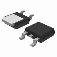
... R 72 qJA R 100 qJA T 260 °C L NID9N05CLT4 NID9N05CLT4G 2 ). NID9N05CL NID9N05CLG †For information on tape and reel specifications, including part orientation and tape sizes, please refer to our Tape and Reel Packaging Specification Brochure, BRD8011/D. 1 http://onsemi.com V I MAX DSS D (Limited) R TYP DS(ON) ...
Page 2
ELECTRICAL CHARACTERISTICS Characteristic OFF CHARACTERISTICS Drain−to−Source Breakdown Voltage (Note 1.0 mA 25° 1.0 mA −40°C to 125° ...
Page 3
ELECTRICAL CHARACTERISTICS Characteristic SWITCHING CHARACTERISTICS (Note 4) Turn−On Delay Time Rise Time Turn−Off Delay Time Fall Time Turn−On Delay Time Rise Time Turn−Off Delay Time Fall Time Turn−On Delay Time Rise Time Turn−Off Delay Time Fall Time Gate Charge (V ...
Page 4
6 DRAIN−TO−SOURCE VOLTAGE (VOLTS) DS Figure 1. On−Region Characteristics 0.5 0.4 0.3 ...
Page 5
TOTAL GATE CHARGE (nC) g Figure 8. Gate−To−Source and Drain−To−Source Voltage versus ...
Page 6
The Forward Biased Safe Operating Area curves define the maximum simultaneous drain−to−source voltage and drain current that a transistor can handle safely when it is forward biased. Curves are based upon maximum peak junction temperature and a case temperature (T ...
Page 7
... V 0.035 0.050 0.89 1.27 Z 0.155 −−− 3.93 −−− STYLE 2: PIN 1. GATE 2. DRAIN 3. SOURCE 4. DRAIN mm inches ON Semiconductor Website: http://onsemi.com Order Literature: http://www.onsemi.com/litorder For additional information, please contact your local Sales Representative. NID9N05CL/D ...