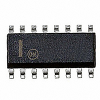
NCP1650DR2 ON Semiconductor, NCP1650DR2 Datasheet - Page 18

NCP1650DR2
Manufacturer Part Number
NCP1650DR2
Description
IC CTRLR PWR FACTOR PWM 16SOIC
Manufacturer
ON Semiconductor
Datasheet
1.NCP1650DR2G.pdf
(31 pages)
Specifications of NCP1650DR2
Mode
Continuous Conduction (CCM), Discontinuous Conduction (DCM)
Frequency - Switching
100kHz
Voltage - Supply
10 V ~ 20 V
Operating Temperature
-40°C ~ 125°C
Mounting Type
Surface Mount
Package / Case
16-SOIC (3.9mm Width)
Switching Frequency
25 KHz to 250 KHz
Maximum Operating Temperature
+ 125 C
Mounting Style
SMD/SMT
Minimum Operating Temperature
- 40 C
Lead Free Status / RoHS Status
Contains lead / RoHS non-compliant
Current - Startup
-
Lead Free Status / Rohs Status
Lead free / RoHS Compliant
Other names
NCP1650DR2OSTR
Available stocks
Company
Part Number
Manufacturer
Quantity
Price
Part Number:
NCP1650DR2G
Manufacturer:
ON/安森美
Quantity:
20 000
recommended that an external resistor be used at the “Ref
Gain” pin, due to tolerance variations of the internal
resistances.
Voltage/Power ORing network. This circuit also limits the
maximum input signal (from the error amplifier) to 3 volts.
voltage- -to- -current converter on the power multiplier. The
current output of the current sense amplifier is used for the
analog input with no scaling.
as an external capacitor. The value of the resistor at pin 9
(max power) will depend on the value of the resistor used at
pin 10 for the current gain and the maximum desired output
power of the converter. These resistors should be the same
style of resistor and have the same temperature coefficients
for best performance.
external components on this multiplier as well as the current
sense amplifier. The current sense amplifier output that
drives the power multiplier has its gain controlled by R
R
the high frequency content from the inductor current signal.
follows:
(1.) V 9 = I CS × R 9 × (V ac ∕V ramp )
Where:
I
sense amplifier
R
V
V
and,
(2.) I CS = V CS × 15∕R 10
frequency we can ignore the effects of the capacitor on this
pin. V
multiplier:
(3.) V 9 =
multiplier, where the inputs are the AC fullwave rectified
sinewave and the current sense input signal.
CS
ac
10
9
ramp
The voltage- -to- -current conversion is performed in the
Power Multiplier/Current Sense Amplifier There is no
The power multiplier requires an external resistor as well
The gain of the power multiplier is based on the values of
The gain for the power multiplier can be calculated as
Since the pole at pin 12 is much greater than twice the line
Equations 1 and 2 can be rearranged to give the gain of the
This gain equation gives the output voltage of the
is the resistor value at pin 9 (Ohms)
, and is filtered by a capacitor on pin 11 which removes
is the rms value of the average current out of the current
is the rms voltage at pin 5
CS
is the sawtooth p- -p ramp voltage (4.0 volts)
is the differential current sense rms input voltage.
3.75 ⋅ R 9 ⋅ V CS ⋅ V ac
R 10
http://onsemi.com
9
and
18
Error Amplifier for ESD protection. Due to this resistor, the
voltage on pin 4 will exceed 4.5 volts under some conditions,
but the maximum voltage at the non- -inverting AC Error
Amplifier input will be clamped at 4.5 volts.
Feedback/Shutdown
function is to provide an input to the error amplifier for
sensing of the output voltage. The signal at this pin is also
sensed by an internal comparator that will shutdown the unit
if the voltage falls below 0.75 volts.
non- -inverting input of the voltage loop error amp. The other
input of the error amp is connected to the internal 4.0 volt
reference. The output of a voltage divider from the high
voltage DC output to ground, feeds this pin.
including overvoltage, undervoltage or hot- -swap control.
An external transistor, open collector or open drain gate,
connected to this pin can be used to pull it low, which will
inhibit the operation of the chip, and change the operating
state to a low power standby mode. An example of a
shutdown circuit is shown in Figure 36.
line conditions the unit will be on. At startup, the AC line is
rectified and charges up the output capacitor. Under normal
line conditions, the output voltage will be great enough to
apply more than 1.0 volt to this pin and the circuit will
commence switching. If the unit is turned on into a low line
condition, the voltage at this pin will not allow the unit to
start.
disable the shutdown function. Both of these circuits limit
the minimum voltage that can appear at the FB/SD input
when the chip is properly biased, while not interfering with
the 4.0 volt level that pin 6 sees when the unit is operating
properly.
Ramp Compensation
compensation to be adjusted for optimum performance.
Ramp compensation is necessary in a current mode
There is a 1 k resistor between the AC Ref pin and the AC
The FB/SD pin is a multiple function pin. Its primary
The feedback circuit applies the signal to the
The shutdown function can be used for multiple purposes
The shutdown circuit is designed such that under normal
Figures 33 and 34 shown circuits that can be used to
The Ramp Compensation pin allows the amount of ramp
Figure 35. Reference Multiplier Clamp Circuit
AC Ref
1 k
Multiplier
25 k
4.5 V
+
--
AC Error
Amplifier


