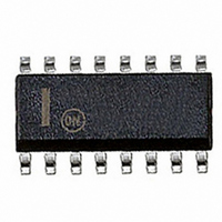
NCP1650DR2 ON Semiconductor, NCP1650DR2 Datasheet - Page 20

NCP1650DR2
Manufacturer Part Number
NCP1650DR2
Description
IC CTRLR PWR FACTOR PWM 16SOIC
Manufacturer
ON Semiconductor
Datasheet
1.NCP1650DR2G.pdf
(31 pages)
Specifications of NCP1650DR2
Mode
Continuous Conduction (CCM), Discontinuous Conduction (DCM)
Frequency - Switching
100kHz
Voltage - Supply
10 V ~ 20 V
Operating Temperature
-40°C ~ 125°C
Mounting Type
Surface Mount
Package / Case
16-SOIC (3.9mm Width)
Switching Frequency
25 KHz to 250 KHz
Maximum Operating Temperature
+ 125 C
Mounting Style
SMD/SMT
Minimum Operating Temperature
- 40 C
Lead Free Status / RoHS Status
Contains lead / RoHS non-compliant
Current - Startup
-
Lead Free Status / Rohs Status
Lead free / RoHS Compliant
Other names
NCP1650DR2OSTR
Available stocks
Company
Part Number
Manufacturer
Quantity
Price
Part Number:
NCP1650DR2G
Manufacturer:
ON/安森美
Quantity:
20 000
Error Amplifiers
regulate the DC output voltage, the maximum output power,
and shape the AC reference fullwave rectified sinewave
signal.
Transconductance amplifiers differ from voltage amplifiers
in that the output is a high impedance with a controlled
voltage- -to- -current gain (i.e. the output current is
proportional to the differential input voltage). The gain of a
transconductance amplifier is determined by the equation:
bandwidth amplifier, which is referred to simply as “Error
Amp” on the block diagram. This amplifier compares the
output DC voltage to the 4.0 volt reference and generates an
error signal which is used to adjust the AC reference voltage
from the reference multiplier.
100 umhos (or 0.0001 amps/volt). This means that an input
voltage differential of 10 mv would cause the output current
to change by 1.0 mA. The maximum output current for this
amplifier in its normal operating range is 50 mA.
amplifier, that increases the output current (or gain) when
the differential input voltage exceeds the reference voltage
by +6% or - -8% the output current is increased to 250 or
–300 mA respectively. This boost circuit allows for rapid
changes to line or load transients by increasing the dv/dt of
the output capacitance of the amplifier.
bandwidth error amplifier which is referred to as the “Power
Amp”. This amplifier performs a similar function to the
Error Amp, only it generates an error signal that holds the
power to a constant level.
100 umhos (or 0.0001 amps/volts). The maximum output
current for this amplifier in its normal operating range is
20 mA. It is also a switched gain transconductance amplifier
similar to the voltage error amplifier, however, the
thresholds are different.
error amp”. It requires a higher bandwidth than the voltage
or power error amplifiers. This amplifier forces a signal
which is the sum of the current and input voltage to equal the
AC reference signal from the reference multiplier.
(or 0.0001 amps/volt). The maximum output current for this
amplifier in its normal operating range is 20 mA. This
The NCP1650 has three error amplifiers. These amplifiers
All three of these are transconductance amplifiers.
Voltage Error Amplifier The voltage loop has a low
The voltage error amplifier has a nominal gain of
This amplifier is a switched gain transconductance
Power Error Amplifier The power loop has a low
The power error amplifier has a nominal gain of
AC Error Amplifier The third error amplifier, is the “AC
The AC error amplifier has a nominal gain of 100 umhos
Av = g m R L
http://onsemi.com
20
amplifier does not contain a boost circuit, and has a constant
transconductance across its operating range.
Voltage and Power ORing Network
are inverting transconductance amplifiers. The network uses
an internal reference of approximately 3.0 volts. Its gain is:
of the current mirror.
voltage will control the loop, as the buffer transistor from the
other amplifier will be in cutoff. As the output voltage of an
amplifier increases, it’s contribution to the current sink will
increase, and the current driving the current mirror will
decrease, thus the output of the current mirror will decrease.
reference multiplier.
Overvoltage Comparator
reduced, the output voltage will overshoot. This circuit, will
minimize the overshoot, and effectively decrease the
response time of the loop.
and shut down the PWM in the event that the output exceeds
8% of the designed output voltage. The feedback voltage is
supplied to this comparator from pin 6, which is the same
signal that the voltage error amplifier uses to regulate the DC
voltage loop.
FB/SD
COMP
6
8
The ORing network for the voltage and power amplifiers
Where the 12.5 k is the internal resistor, and 4 is the gain
The amplifier (voltage or power) with the highest output
The current mirror output feeds the analog (a) input to the
For a load transient, in which the current is suddenly
A comparator is provided to monitor the feedback voltage
+
--
+
--
VOLTAGE
POWER
Figure 37. Voltage/Power ORing Network
AMP
V
I out = (V ref − V in) ·
AMP
in
12.5 k
12.5 k
4
CURRENT
=
MIRROR
i
3 V − V in
3,125
3.0 V
Reference
Multiplier,
Input a
To
4
i


