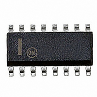
NCP1650DR2 ON Semiconductor, NCP1650DR2 Datasheet - Page 25

NCP1650DR2
Manufacturer Part Number
NCP1650DR2
Description
IC CTRLR PWR FACTOR PWM 16SOIC
Manufacturer
ON Semiconductor
Datasheet
1.NCP1650DR2G.pdf
(31 pages)
Specifications of NCP1650DR2
Mode
Continuous Conduction (CCM), Discontinuous Conduction (DCM)
Frequency - Switching
100kHz
Voltage - Supply
10 V ~ 20 V
Operating Temperature
-40°C ~ 125°C
Mounting Type
Surface Mount
Package / Case
16-SOIC (3.9mm Width)
Switching Frequency
25 KHz to 250 KHz
Maximum Operating Temperature
+ 125 C
Mounting Style
SMD/SMT
Minimum Operating Temperature
- 40 C
Lead Free Status / RoHS Status
Contains lead / RoHS non-compliant
Current - Startup
-
Lead Free Status / Rohs Status
Lead free / RoHS Compliant
Other names
NCP1650DR2OSTR
Available stocks
Company
Part Number
Manufacturer
Quantity
Price
Part Number:
NCP1650DR2G
Manufacturer:
ON/安森美
Quantity:
20 000
Current Sense Resistor/Ramp Compensation
current sense resistor and ramp compensation signal, will
determine the peak instantaneous current that the power
switch will be allowed to conduct before it is turned off.
the signal at the non- -inverting input to the PWM comparator
must add up to 4.0 volts in order to terminate the switch
cycle. These signals are the error signal from the AC error
amp, the ramp compensation signal, and the instantaneous
current. For a worst case condition, the output of the AC
error amp could be zero (current), which would require that
the sum of the ramp compensation signal and current signal
be 4.0 volts. This must be evaluated under full load and low
line conditions.
Equation 1)
Where: V
match the falling di/dt (which has been converted to a dv/dt)
of the inductor at 50% duty cycle. 50% duty cycle will occur
when the input voltage is 50% of the output voltage. Thus the
following equations must be satisfied:
Equation 2)
R
P
L = Inductance (H)
Where: t
T = Period (s)
Vin
Vout = DC output voltage (V)
O
S
The combination of the voltage developed across the
The vector sum of the three signals that combine to create
For proper ramp compensation, the ramp signal should
= Shunt resistance (Ω)
= Output power (W)
LL
= Low line input voltage (Vrms)
dt
V o * T * R S * 16
R S =
di
on
V RCOMP =
oscpk
* T * R S * High Frequency Current Gain
= Switch on time (s)
V RCOMP =
V o * T * R RC
L * 2
i pk =
= 4.0 V
t on = T
12800 * L
⋅ P
2
Vin LL
1.6 * 4 * 16 k
1.6 * V oscpk * 16 k
1 −
=
R RC
in
+
102, 400
· Vin
2
R RC
Vin LL ⋅ t on
V out
R RC
⋅ L
2
=
LL
102, 400
R RC
http://onsemi.com
25
Ramp Compensation:
Equation 3)
Where: V
Where:
R
L = Inductance (H)
V
R
Current Shunt:
Equation 4)
Combining equations 2 and 3:
should be understood that these equations do not take into
account tolerances of the inductor, switching frequency, etc
type of resistor. There are several types of metal film
resistors available for shunt applications.
Current Scaling Resistor and Filter Capacitor
current sense amplifier. This signal is fed into the AC error
amplifier and is also used in the power multiplier. R
to scale the current to the appropriate level for protection
purposes in the AC error amplifier circuit. The power
multiplier has an external resistor, R
of that circuit.
signal at the input to the AC error amplifier to less than
4.5 volts at low line and full load. 4.5 volts is the clamp
voltage at the output of the reference amplifier and limits the
maximum averaged current that the unit can process. The
equation for R
Where:
Pin = rated input power (w)
R
Vin
AC
out
S
RC
S
R S =
R S =
Solve for R
The shunt should be a non- -wirewound (low inductance)
R
R
= Shunt resistance (Ω)
= Shunt resistance (W)
ratio
LL
10
10
= Output voltage (V)
= Ramp comp resistor (kΩ)
sets the gain of the averaged current signal out of the
should be calculated to limit the maximum current
= min. operating rms input voltage (v)
= AC attenuation factor at pin 5
3.8 = (i pk * R S * 16 +
R RC =
V o * T * R RC
refpwm
8 * V o * t on
R 10 =
12800 * L
L
S
V refpwm = V inst + V RCOMP
10
and then R
= 3.8 V
(3.8 − (16 * i pk * R S ))
is:
4.5 − (1.06 · Vin LL · AC ratio )
3.8
+
318, 200 · P in · R S ∕Vin LL
16 * i pk
102, 400
* T
RC
t on *
, using the above equations. It
(3.8 − 16 * i pk * R S )
102, 400
9
R RC
that will adjust the gain
102, 400
*
) *
t on
T
t on
T
10
is used


