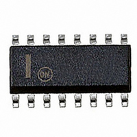
NCP1650DR2 ON Semiconductor, NCP1650DR2 Datasheet - Page 28

NCP1650DR2
Manufacturer Part Number
NCP1650DR2
Description
IC CTRLR PWR FACTOR PWM 16SOIC
Manufacturer
ON Semiconductor
Datasheet
1.NCP1650DR2G.pdf
(31 pages)
Specifications of NCP1650DR2
Mode
Continuous Conduction (CCM), Discontinuous Conduction (DCM)
Frequency - Switching
100kHz
Voltage - Supply
10 V ~ 20 V
Operating Temperature
-40°C ~ 125°C
Mounting Type
Surface Mount
Package / Case
16-SOIC (3.9mm Width)
Switching Frequency
25 KHz to 250 KHz
Maximum Operating Temperature
+ 125 C
Mounting Style
SMD/SMT
Minimum Operating Temperature
- 40 C
Lead Free Status / RoHS Status
Contains lead / RoHS non-compliant
Current - Startup
-
Lead Free Status / Rohs Status
Lead free / RoHS Compliant
Other names
NCP1650DR2OSTR
Available stocks
Company
Part Number
Manufacturer
Quantity
Price
Part Number:
NCP1650DR2G
Manufacturer:
ON/安森美
Quantity:
20 000
in the introduction to this analysis, this is not analyzed
separately.
the pole. There is a single pole due to the output filter. Since
the NCP1650 is a current mode converter, the inductor is not
part of the output pole as can be seen in that equation.
Calculating the Loop Gain
involved in this calculation have been determined with the
exception of the pole- -zero pair on the output of the voltage
error amplifier.
necessary to convert these to the decibel format using the
following formula:
For example, the voltage divider would be:
It is recommended that the compensation for the voltage
error amplifier be calculated under high line, full load
conditions. This should be the greatest bandwidth that the
unit will see.
PFC unit, must be less than the line frequency. If the
bandwidth approaches or exceeds the line frequency, the
voltage error amplifier signal will have frequency
components in its output that are greater than the line
frequency. These components will cause distortion in the
output of the reference amplifier, which is used to shape the
current waveform. This in turn will cause distortion in the
current and reduce the power factor.
converter is 10 Hz, and slightly less for a 50 Hz system. This
can be adjusted to meet the particular requirements of a
system. The unity gain bandwidth is determined by the
frequency at which the loop gain passes through the 0 dB
level.
with a slope of –20 dB/decade for approximately one decade
on either side of the unity gain frequency. This assures a
phase margin of greater than 45.
of Figure 43 as follows:
it will not change with frequency.
of the AC input signal at high line that will be seen on pin 5.
Convert this to dB. This is also a constant value.
DVo/DVref. Calculate the pole frequency. The gain will be
constant for all frequencies less than f
frequency, this gain will drop off at a rate of 20 dB/decade.
The equation for the gain is good for frequencies below
At this point in the design process, all of the parameters
All equations give gains in absolute numbers. It is
The gain of the loop will vary as the input voltage changes.
By necessity, the unity gain (OdB) loop bandwidth for a
Typically the maximum bandwidth for a 60 Hz PFC
For stability purposes, the gain should pass through 0 dB
The gain can be calculated graphically using the equations
Divider: Calculate V’/Vo in dB, this value is constant so
Reference Signal: Calculate V
Modulator and Output Stage: Calculate the gain in dB for
A(dB) = 20 Log 10 .0099 = − 40 dB
A =
A(dB) = 20 Log 10 (A)
560 k + 5.6 k
5.6 k
ref
/V
= .0099
e/a
p
. Starting at the pole
using the peak level
http://onsemi.com
28
of 35.5 dB until the pole of the output filter is reached at
0.3 Hz. After that, the gain is reduced at a rate of
20 dB/decade.
The zero is used to offset the pole of the output filter. The
output filter pole will typically be lower than the unity gain
loop bandwidth, so the zero will be necessary.
compensate for this the error amplifier should have a gain of
–7.0 dB (0.45) at 10 Hz, and a zero at 0.4 Hz. The gain at
10 Hz is determined by the resistor since it is well past the
zero. The resistor can be calculated by the equation:
capacitor can be calculated based on the zero frequency of
0.4 Hz. This would give a value for C
Using these values (4.7 kΩ and 86 mF), the open loop gain
plot would be:
--10
--20
--30
--40
--20
--40
Plot the sum of these three values. Figure 43 shows a gain
A typical error amplifier bode plot is shown in Figure 44.
This plot shows a forward gain of 7.0 dB at 10 Hz. To
4.7 kW is the closest standard value. Using this, the
40
30
20
10
80
60
40
20
0
0
0.01
0.01
Figure 44. Open Loop Gain of Voltage Loop
Figure 43. Open Loop Gain Less Error Amp
R 7 = A v ∕G m = .45∕.0001 = 4.5 kΩ
C =
0.1
0.1
2 ⋅ π ⋅ 4.7 k ⋅ 0.4 Hz
FREQUENCY (Hz)
FREQUENCY (Hz)
1
1
1
10
10
7
of:
= 85 mF
ERROR AMP
LOOP BODE
LOOP GAIN
WITHOUT
VOLTAGE
PLOT
100
100
1000
1000


