MCP1525T-I/TT Microchip Technology, MCP1525T-I/TT Datasheet - Page 9
MCP1525T-I/TT
Manufacturer Part Number
MCP1525T-I/TT
Description
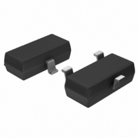
IC VOLT REF 2.5V SOT23-3
Manufacturer
Microchip Technology
Datasheet
1.MCP1525T-ITT.pdf
(20 pages)
Specifications of MCP1525T-I/TT
Reference Type
Series
Package / Case
SOT-23-3, TO-236-3, Micro3™, SSD3, SST3
Voltage - Output
2.5V
Tolerance
±1%
Temperature Coefficient
50ppm/°C
Voltage - Input
2.7 ~ 5.5 V
Number Of Channels
1
Current - Quiescent
100µA
Current - Output
2mA
Operating Temperature
-40°C ~ 85°C
Mounting Type
Surface Mount
Product
Voltage References
Topology
Series References
Output Voltage
2.5 V
Initial Accuracy
1 %
Average Temperature Coefficient (typ)
50 ppm/C
Series Vref - Input Voltage (max)
7 V
Series Vref - Input Voltage (min)
2.7 V
Shunt Current (max)
8 mA (Typ)
Maximum Operating Temperature
+ 85 C
Input Voltage
5.5 V
Minimum Operating Temperature
- 40 C
Mounting Style
SMD/SMT
Series Vref - Supply Current (max)
100 uA
Lead Free Status / RoHS Status
Lead free / RoHS Compliant
Current - Cathode
-
Lead Free Status / Rohs Status
Lead free / RoHS Compliant
Other names
MCP1525T-I/TT
MCP1525T-I/TTTR
MCP1525TI/TT
MCP1525T-I/TTTR
MCP1525TI/TT
Available stocks
Company
Part Number
Manufacturer
Quantity
Price
Company:

Part Number:
MCP1525T-I/TT
Manufacturer:
LT
Quantity:
3 400
Part Number:
MCP1525T-I/TT
Manufacturer:
MICROCHIP/微芯
Quantity:
20 000


4.0
4.1
4.1.1
The MCP1525 and MCP1541 voltage reference
devices should be applied as shown in Figure 4-1 in all
applications.
FIGURE 4-1:
As shown in Figure 4-1, the input voltage is connected
to the device at the V
ceramic capacitor. This capacitor would be required if
the input voltage has excess noise. A 0.1 µF capacitor
would reject input voltage noise at approximately
1 to 2 MHz. Noise below this frequency will be amply
rejected by the input voltage rejection of the voltage ref-
erence. Noise at frequencies above 2 MHz will be
beyond the bandwidth of the voltage reference and,
consequently, not transmitted from the input pin
through the device to the output.
The load capacitance (C
stabilize the voltage reference; see Section 4.1.3
“Load Capacitor”.
4.1.2
The MCP1525 and MCP1541 voltage references do
not require an input capacitor across V
However, for added stability and input voltage transient
noise reduction, a 0.1 µF ceramic capacitor is
recommended, as shown in Figure 4-1. This capacitor
should be close to the device (within 5 mm of the pin).
4.1.3
The output capacitor from V
frequency compensation for the references and cannot
be omitted. Use load capacitors between 1 µF and
10 µF to compensate these devices. A 10 µF output
capacitor has slightly better noise, and provides
additional charge for fast load transients, when
compared to a 1 µF output capacitor. This capacitor
should be close to the device (within 5 mm of the pin).
© 2005 Microchip Technology Inc.
V
REF
APPLICATIONS INFORMATION
Application Tips
BASIC CIRCUIT CONFIGURATION
INPUT (BYPASS) CAPACITOR
LOAD CAPACITOR
(optional)
0.1 µF
C
IN
IN
Basic Circuit Configuration.
V
input, with an optional 0.1 µF
DD
L
) is required in order to
C
1 µF to 10 µF
L
OUT
MCP1525
MCP1541
V
V
IN
OUT
to V
V
SS
SS
IN
acts as a
to V
SS
.
4.1.4
Mechanical stress due to Printed Circuit Board (PCB)
mounting can cause the output voltage to shift from its
initial value. Devices in the SOT-23-3 package are
generally more prone to assembly stress than devices
in the TO-92 package. To reduce stress-related output
voltage shifts, mount the reference on low-stress areas
of the PCB (i.e., away from PCB edges, screw holes
and large components).
4.1.5
If the noise at the output of these voltage references is
too high for the particular application, it can be easily
filtered with an external RC filter and op amp buffer.
The op amp’s input and output voltage ranges need to
include the reference output voltage.
FIGURE 4-2:
Filter.
The RC filter values are selected for a desired cutoff
frequency:
EQUATION 4-1:
The values that are shown in Figure 4-2 (10 k
1 µF) will create a first-order, low-pass filter at the
output of the amplifier. The cutoff frequency of this filter
is 15.9 Hz, and the attenuation slope is 20 dB/decade.
The MCP6021 amplifier isolates the loading of this low-
pass filter from the remainder of the application circuit.
This amplifier also provides additional drive, with a
faster response time than the voltage reference.
V
V
V
V
OUT
DD
SS
IN
MCP1525
MCP1541
PRINTED CIRCUIT BOARD LAYOUT
CONSIDERATIONS
OUTPUT FILTERING
C
10 µF
10 kW
L
R
f
C
FIL
=
MCP1525/41
Output Noise-Reducing
------------------------------
2 R
C
1 µF
FIL
1
FIL
C
FIL
MCP6021
V
DS21653B-page 9
DD
V
REF
and
Related parts for MCP1525T-I/TT
Image
Part Number
Description
Manufacturer
Datasheet
Request
R

Part Number:
Description:
2.5V and 4.096V Voltage References
Manufacturer:
Microchip Technology
Datasheet:

Part Number:
Description:
IC VOLTAGE REFERENCE 2.5V TO92-3
Manufacturer:
Microchip Technology
Datasheet:
Part Number:
Description:
MCP1525 is a low power, high precision voltage reference. It provides a precise output voltage of 2.5V which is then compared to ...
Manufacturer:
Microchip Technology
Part Number:
Description:
Precision Voltage Reference
Manufacturer:
Microchip Technology
Datasheet:
Part Number:
Description:
2.5V and 4.096V Voltage References
Manufacturer:
Microchip Technology
Datasheet:

Part Number:
Description:
Manufacturer:
Microchip Technology Inc.
Datasheet:
Part Number:
Description:
Manufacturer:
Microchip Technology Inc.
Datasheet:
Part Number:
Description:
Manufacturer:
Microchip Technology Inc.
Datasheet:
Part Number:
Description:
Manufacturer:
Microchip Technology Inc.
Datasheet:
Part Number:
Description:
Manufacturer:
Microchip Technology Inc.
Datasheet:
Part Number:
Description:
Manufacturer:
Microchip Technology Inc.
Datasheet: