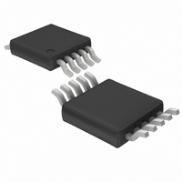
LTC3440EMS Linear Technology, LTC3440EMS Datasheet - Page 9

LTC3440EMS
Manufacturer Part Number
LTC3440EMS
Description
IC DC/DC CONV BUCK-BOOST 10-MSOP
Manufacturer
Linear Technology
Type
Step-Down (Buck), Step-Up (Boost)r
Datasheet
1.LTC3440EMS.pdf
(20 pages)
Specifications of LTC3440EMS
Internal Switch(s)
Yes
Synchronous Rectifier
Yes
Number Of Outputs
1
Voltage - Output
2.5 ~ 5.5 V
Current - Output
600mA
Frequency - Switching
2MHz
Voltage - Input
2.5 ~ 5.5 V
Operating Temperature
-40°C ~ 85°C
Mounting Type
Surface Mount
Package / Case
10-MSOP, Micro10™, 10-uMAX, 10-uSOP
Lead Free Status / RoHS Status
Contains lead / RoHS non-compliant
Power - Output
-
Available stocks
Company
Part Number
Manufacturer
Quantity
Price
Company:
Part Number:
LTC3440EMS
Manufacturer:
LT
Quantity:
5 321
Company:
Part Number:
LTC3440EMS
Manufacturer:
LT
Quantity:
2 500
Part Number:
LTC3440EMS
Manufacturer:
LT/凌特
Quantity:
20 000
Part Number:
LTC3440EMS#PBF
Manufacturer:
LINEAR/凌特
Quantity:
20 000
Company:
Part Number:
LTC3440EMS#TR
Manufacturer:
LT
Quantity:
3 000
Part Number:
LTC3440EMS#TR
Manufacturer:
LT/凌特
Quantity:
20 000
Company:
Part Number:
LTC3440EMS#TRPBF
Manufacturer:
MSC
Quantity:
45
Company:
Part Number:
LTC3440EMS#TRPBF
Manufacturer:
LT
Quantity:
5 510
Part Number:
LTC3440EMS#TRPBF
Manufacturer:
LINEAR/凌特
Quantity:
20 000
OPERATIO
Buck Region (V
Switch D is always on and switch C is always off during this
mode. When the internal control voltage, V
voltage V1, output A begins to switch. During the off time
of switch A, synchronous switch B turns on for the
remainder of the time. Switches A and B will alternate
similar to a typical synchronous buck regulator. As the
control voltage increases, the duty cycle of switch A
increases until the maximum duty cycle of the converter in
Buck mode reaches D
where D4
where f = operating frequency, Hz.
Beyond this point the “four switch,” or Buck/Boost region
is reached.
Buck/Boost or Four Switch (V
When the internal control voltage, V
switch pair AD remain on for duty cycle D
the switch pair AC begins to phase in. As switch pair AC
phases in, switch pair BD phases out accordingly. When
the V
at voltage V3, the AC switch pair completely phase out the
BD pair, and the boost phase begins at duty cycle D4
D4
D
Figure 2. Switch Control vs Internal Control Voltage, V
BOOST
BOOST
CYCLE
MAX
CI
D
D
BUCK
DUTY
SW
D
75%
MAX
MAX
MIN
0%
voltage reaches the edge of the Buck/Boost range,
_
= (150ns • f) • 100 %
SW
BUCK
PWM CD SWITCHES
FOUR SWITCH PWM
PWM AB SWITCHES
= duty cycle % of the four switch range.
A ON, B OFF
D ON, C OFF
= 100 – D4
IN
U
> V
OUT
MAX
BOOST REGION
BUCK REGION
)
_
SW
BUCK
%
IN
BUCK/BOOST REGION
, given by:
~ V
CI
OUT
, is above voltage V2,
)
MAX_BUCK
3440 F02
CI
, is above
V4 (≈2.05V)
V3 (≈1.65V)
V2 (≈1.55V)
V1 (≈0.9V)
INTERNAL
CONTROL
VOLTAGE, V
CI
, and
SW
CI
.
The input voltage, V
is given by:
The point at which the four switch region ends is given by:
Boost Region (V
Switch A is always on and switch B is always off during
this mode. When the internal control voltage, V
voltage V3, switch pair CD will alternately switch to
provide a boosted output voltage. This operation is typical
to a synchronous boost regulator. The maximum duty
cycle of the converter is limited to 75% typical and is
reached when V
Burst Mode Operation
Burst Mode operation is when the IC delivers energy to the
output until it is regulated and then goes into a sleep mode
where the outputs are off and the IC is consuming only
25μA. In this mode the output ripple has a variable
frequency component that depends upon load current.
During the period where the device is delivering energy to
the output, the peak current will be equal to 400mA typical
and the inductor current will terminate at zero current for
each cycle. In this mode the maximum average output
current is given by:
Burst Mode operation is user controlled, by driving the
MODE/SYNC pin high to enable and low to disable.
The peak efficiency during Burst Mode operation is less
than the peak efficiency during fixed frequency because
the part enters full-time 4-switch mode (when servicing
the output) with discontinuous inductor current as illus-
trated in Figures 3 and 4. During Burst Mode operation, the
control loop is nonlinear and cannot utilize the control
V
I
V
OUT MAX BURST
IN
IN
= V
=
(
1 150
OUT
– (
)
V
(1 – D) = V
OUT
CI
IN
ns f
is above V4.
IN
< V
≈
• )
, where the four switch region begins
V
OUT
OUT
V
0 1
. •
OUT
)
+
(1 – 150ns • f) V
V
IN
V
IN
A
LTC3440
CI
, is above
3440fb
9


