LTC3602EUF#PBF Linear Technology, LTC3602EUF#PBF Datasheet
LTC3602EUF#PBF
Specifications of LTC3602EUF#PBF
Available stocks


Related parts for LTC3602EUF#PBF


LTC3602EUF#PBF Summary of contents
Page 1
FEATURES n Wide Input Voltage Range: 4.5V to 10V n 2.5A Output Current n Low R Internal Switches: 65mΩ and 90mΩ DS(ON) n Programmable Frequency: 300kHz to 3MHz n Low Quiescent Current: 75μA n 0.6V ±1% Reference Allows Low Output ...
Page 2
... TAPE AND REEL LTC3602EFE#PBF LTC3602EFE#TRPBF LTC3602IFE#PBF LTC3602IFE#TRPBF LTC3602EUF#PBF LTC3602EUF#TRPBF LTC3602IUF#PBF LTC3602IUF#TRPBF Consult LTC Marketing for parts specifi ed with wider operating temperature ranges. *The temperature grade is identifi label on the shipping container. Consult LTC Marketing for information on non-standard lead based fi nish parts. ...
Page 3
ELECTRICAL CHARACTERISTICS temperature range, otherwise specifi cations are at T SYMBOL PARAMETER ΔV Power Good Range PGOOD R Power Good Resistance PGOOD I FB Input Bias Current FB g Transconductance Amplifi Supply Current S Active Mode ...
Page 4
LTC3602 TYPICAL PERFORMANCE CHARACTERISTICS V vs Temperature REF 0.6008 V = 8.4V IN 0.6006 0.6004 0.6002 0.6000 0.5998 0.5996 –50 – 100 TEMPERATURE (°C) 3602 G03 PV Leakage Current IN vs Input Voltage ...
Page 5
TYPICAL PERFORMANCE CHARACTERISTICS Minimum Peak Inductor Current vs Burst Clamp Voltage 3.0 2.5 2.0 1.5 1.0 0.5 0 0.4 0.5 0.6 0.7 0.8 0.9 BURST CLAMP VOLTAGE (V) 3602 G12 Effi ciency vs Load Current, Forced Continuous 100 FIGURE 6 ...
Page 6
LTC3602 PIN FUNCTIONS FE/UF Package SYNC/MODE (Pin 1/Pin 4): Mode Select and External Clock Synchronization Input. PGOOD (Pin 2/Pin 5): Power Good Output. Open-drain logic output that is pulled to ground when the output volt- age is not within ±10% ...
Page 7
OPERATION Main Control Loop The LTC3602 is a monolithic, constant-frequency, current- mode step-down DC/DC converter. During normal opera- tion, the internal top power switch (N-channel MOSFET) is turned on at the beginning of each clock cycle. Current in the inductor ...
Page 8
LTC3602 OPERATION Dropout Operation When the input supply voltage decreases toward the output voltage, the duty cycle increases toward the maximum on-time. Further reduction of the supply voltage forces the top switch to remain on for more than one cycle ...
Page 9
APPLICATIONS INFORMATION The basic LTC3602 application circuit is shown on the front page of this data sheet. External component selection is determined by the maximum load current and begins with the selection of the inductor value and operating frequency followed ...
Page 10
LTC3602 APPLICATIONS INFORMATION characteristics. The choice of which style inductor to use mainly depends on the price vs size requirements and any radiated fi eld/EMI requirements. New designs for surface mount inductors are available from Coiltronics, Coilcraft, Toko and Sumida. ...
Page 11
APPLICATIONS INFORMATION Burst Clamp Programming If the voltage on the SYNC/MODE pin is less than INTV more, Burst Mode operation is enabled. During Burst Mode operation, the voltage on the SYNC/MODE pin determines the burst clamp level. ...
Page 12
LTC3602 APPLICATIONS INFORMATION Topside MOSFET Driver Supply (BOOST Pin) The LTC3602 uses a bootstrapped supply to power the gate of the internal topside MOSFET (Figure 3). When the topside MOSFET is off and the SW pin is low, diode D ...
Page 13
APPLICATIONS INFORMATION LTC3602 TRACK/ 3602 F05a Figure 5a. Using the TRACK/SS Pin to Track V TIME (5b) Ratiometric Tracking TIME (5c) Coincident Tracking Effi ciency Considerations The effi ciency of a switching ...
Page 14
LTC3602 APPLICATIONS INFORMATION Thermal Considerations In most applications, the LTC3602 does not dissipate much heat due to its high effi ciency. But, in applications where the LTC3602 is running at high ambient temperature with low supply voltage and high duty ...
Page 15
APPLICATIONS INFORMATION capacitance and a ceramic capacitor in parallel to lower the total effective ESR. For this design, a 100μF ceramic capacitor will be used. C should be sized for a maximum IN current rating of ...
Page 16
LTC3602 TYPICAL APPLICATIONS 845k 200k PGOOD R4 R OSC 137k 105k C ITH R ITH 1nF 4.32k R1 105k 22pF 210k L1: VISHAY IHLP2525CZER1R0MO1 C : TAIYO YUDEN TMK325BJ226MM TAIYO YUDEN AMK316BJ107ML ...
Page 17
TYPICAL APPLICATIONS 3.3V, 2.5A Regulator at 2MHz, Forced Continuous, Small Size R PG 200k PGOOD R OSC 47.5k C ITH R ITH 470pF 2.94k R1 105k 10pF 475k L1: VISHAY IHLP1616ABER1R0M01 C : TAIYO YUDEN EMK316BJ226ML-T IN ...
Page 18
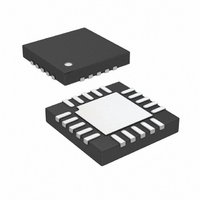
LTC3602 PACKAGE DESCRIPTION 6.60 0.10 4.50 0.10 SEE NOTE 4 RECOMMENDED SOLDER PAD LAYOUT 4.30 – 4.50* (.169 – .177) 0.09 – 0.20 (.0035 – .0079) NOTE: 1. CONTROLLING DIMENSION: MILLIMETERS 2. DIMENSIONS ARE IN 3. DRAWING NOT TO SCALE ...
Page 19
... ON THE TOP AND BOTTOM OF PACKAGE Information furnished by Linear Technology Corporation is believed to be accurate and reliable. However, no responsibility is assumed for its use. Linear Technology Corporation makes no representa- tion that the interconnection of its circuits as described herein will not infringe on existing patent rights. UF Package 20-Lead Plastic QFN (4mm × ...
Page 20
... LTC3548 400mA/800mA Dual Synchronous Buck-Boost DC/DC Converter LTC3610 12A, 24V, Synchronous Step-Down DC/DC Converter LTC3611 10A, 36V, Synchronous Step-Down DC/DC Converter ThinSOT is a trademark of Linear Technology Corporation. Linear Technology Corporation 20 1630 McCarthy Blvd., Milpitas, CA 95035-7417 (408) 432-1900 FAX: (408) 434-0507 ● ...