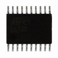
L6730C STMicroelectronics, L6730C Datasheet - Page 32

L6730C
Manufacturer Part Number
L6730C
Description
IC CTRLR ADJ STPDN SYNC 20-TSSOP
Manufacturer
STMicroelectronics
Type
Step-Down (Buck)r
Datasheet
1.L6730DTR.pdf
(50 pages)
Specifications of L6730C
Internal Switch(s)
No
Synchronous Rectifier
Yes
Number Of Outputs
1
Voltage - Output
Adj to 0.6V
Frequency - Switching
100kHz ~ 1MHz
Voltage - Input
1.8 ~ 14 V
Operating Temperature
-40°C ~ 85°C
Mounting Type
Surface Mount
Package / Case
20-TSSOP Exposed Pad, 20-eTSSOP, 20-HTSSOP
Package
HTSSOP20, QFN4x4 24L
For Use With
497-5868 - EVAL BOARD 30A 400KHZ L6730497-5501 - EVAL BOARD FOR L6730XX
Lead Free Status / RoHS Status
Lead free / RoHS Compliant
Current - Output
-
Power - Output
-
Application details
6.4
Figure 26. Compensation network
32/50
Compensation network
The loop is based on a voltage mode control
internal/external reference voltage and scaled by the external resistor divider. The error
amplifier output V
width modulated (PWM) with an amplitude of V
by the output filter. The modulator transfer function is the small signal transfer function of V
V
and a zero at F
simply the input voltage V
The compensation network consists in the internal error amplifier, the impedance networks Z
(R3, R4 and C20) and Z
closed loop transfer function with the highest 0dB crossing frequency to have fastest transient
response (but always lower than f
load regulation error. A stable control loop has a gain crossing the 0dB axis with -20dB/decade
slope and a phase margin greater than 45°. To locate poles and zeroes of the compensation
networks, the following suggestions may be used:
●
●
COMP
Modulator singularity frequencies:
Compensation network singularity frequencies:
. This function has a double pole at frequency F
P
ESR
1
LC
COMP
Z
depending on the output capacitor’s ESR. The DC Gain of the modulator is
1
R
5
is then compared with the oscillator triangular wave to provide a pulse-
R
L
FB
C
5
IN
C
1
1
Cout
(R5, C18 and C19). The compensation network has to provide a
18
1
18
C
divided by the peak-to-peak oscillator voltage: V
19
Z
C
C
FB
19
19
SW
(17)
(13)
/10) and the highest gain in DC conditions to minimize the
(15)
(Figure
ESR
Z
2
IN
P
at the PHASE node. This waveform is filtered
2
C
ESR
20
26.). The output voltage is regulated to the
R
LC
4
1
R
1
Cout
1
depending on the L-Cout resonance
3
C
20
R
4
Z
(16)
(14)
IN
(18)
L6730C - L6730D
OSC
.
OUT
IN
/


