HCPL-3150-000E Avago Technologies US Inc., HCPL-3150-000E Datasheet - Page 13
HCPL-3150-000E
Manufacturer Part Number
HCPL-3150-000E
Description
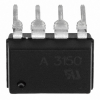
OPTOCOUPLER 1CH 0.6A 8-DIP
Manufacturer
Avago Technologies US Inc.
Datasheet
1.HCPL-3150.pdf
(21 pages)
Specifications of HCPL-3150-000E
Output Type
Open Collector
Package / Case
8-DIP (0.300", 7.62mm)
Voltage - Isolation
3750Vrms
Number Of Channels
1, Unidirectional
Current - Output / Channel
600mA
Propagation Delay High - Low @ If
300ns @ 7mA ~ 16mA
Current - Dc Forward (if)
25mA
Input Type
DC
Mounting Type
Through Hole
Configuration
1 Channel
Isolation Voltage
3750 Vrms
Maximum Propagation Delay Time
500 ns
Maximum Forward Diode Voltage
1.8 V
Minimum Forward Diode Voltage
1.2 V
Maximum Reverse Diode Voltage
5 V
Maximum Forward Diode Current
25 mA
Maximum Power Dissipation
295 mW
Maximum Operating Temperature
+ 100 C
Minimum Operating Temperature
- 40 C
Number Of Elements
1
Forward Voltage
1.8V
Forward Current
25mA
Package Type
PDIP
Operating Temp Range
-40C to 100C
Power Dissipation
295mW
Propagation Delay Time
500ns
Pin Count
8
Mounting
Through Hole
Reverse Breakdown Voltage
5V
Operating Temperature Classification
Industrial
No. Of Channels
1
Optocoupler Output Type
Gate Drive
Input Current
16mA
Output Voltage
30V
Opto Case Style
DIP
No. Of Pins
8
Common Mode Ratio
15 KV/uS
Rohs Compliant
Yes
Lead Free Status / RoHS Status
Lead free / RoHS Compliant
Lead Free Status / RoHS Status
Lead free / RoHS Compliant, Lead free / RoHS Compliant
Other names
516-1742-5
HCPL-3150-000E
HCPL-3150-000E
Available stocks
Company
Part Number
Manufacturer
Quantity
Price
Company:

Part Number:
HCPL-3150-000E
Manufacturer:
AVAGO
Quantity:
20 000
Part Number:
HCPL-3150-000E
Manufacturer:
AVAGO/安华高
Quantity:
20 000


50% DUTY
Figure 23. t
5 V
Figure 24. CMR Test Circuit and Waveforms.
Applications Information
Eliminating Negative IGBT Gate Drive
To keep the IGBT firmly off, the HCPL-3150/315J has a
very low maximum V
3150/315J realizes this very low V
transistor with 4 Ω (typical) on resistance in its pull down
circuit. When the HCPL-3150/315J is in the low state, the
IGBT gate is shorted to the emitter by Rg + 4 Ω. Minimiz-
ing Rg and the lead inductance from the HCPL-3150/315J
to the IGBT gate and emitter (possibly by mounting the
HCPL-3150/315J on a small PC board directly above the
IGBT) can eliminate the need for negative IGBT gate drive
13
Figure 25a. Recommended LED Drive and Application Circuit.
CONTROL
10 KHz
CYCLE
COLLECTOR
INPUT
+
–
I
F
= 7 to 16 mA
+5 V
+
–
I
F
74XXX
OPEN
PLH
500 Ω
, t
A
B
PHL
270 Ω
, t
r
1
2
3
4
1
2
3
4
, and t
f
Test Circuit and Waveforms.
OL
V
1
2
3
4
CM
specification of 1.0 V . The HCPL-
+
= 1500 V
HCPL-3150
OL
by using a DMOS
8
7
6
5
8
7
6
5
0.1 μF
0.1 μF
8
7
6
5
0.1 μF
47 Ω
V
3 nF
O
V
O
+
–
+
–
V
V
CC
to 30 V
CC
+
–
= 30 V
V
= 15
CC
Rg
in many applica tions as shown in Figure 25. Care should
be taken with such a PC board design to avoid routing
the IGBT collector or emitter traces close to the HCPL-
3150/315J input as this can result in unwanted coupling
of transient signals into the HCPL-3150/315J and de-
grade performance. (If the IGBT drain must be routed
near the HCPL-3150/315J input, then the LED should be
reverse-biased when in the off state, to prevent the tran-
sient signals coupled from the IGBT drain from turning
on the HCPL-3150/315J.)
= 18 V
V
0 V
V
SWITCH AT A: I
V
SWITCH AT B: I
Q1
Q2
CM
O
O
I
V
F
OUT
t
PLH
Δt
F
F
t
= 10 mA
= 0 mA
r
3-PHASE
+ HVDC
- HVDC
AC
t
PHL
t
f
90%
50%
10%
δV
δt
=
V
Δt
CM
V
V
OH
OL
Related parts for HCPL-3150-000E
Image
Part Number
Description
Manufacturer
Datasheet
Request
R

Part Number:
Description:
OPTOCOUPLER GATE DRIVE 0.6A 8DIP
Manufacturer:
Avago Technologies US Inc.
Datasheet:

Part Number:
Description:
OPTOCOUPLER 1CH 0.6A 8-SMD
Manufacturer:
Avago Technologies US Inc.
Datasheet:
Part Number:
Description:
OPTOCOUPLER GATE DRIVE 0.6A 8SMD
Manufacturer:
Avago Technologies US Inc.
Datasheet:
Part Number:
Description:
OPTOCOUPLER 1CH 0.6A VDE 8-SMD
Manufacturer:
Avago Technologies US Inc.
Datasheet:

Part Number:
Description:
OPTOCOUPLER 1CH 0.6A IEC 8-SMD
Manufacturer:
Avago Technologies US Inc.
Datasheet:

Part Number:
Description:
OPTOCOUPLER 1CH 0.6A 8-SMD GW
Manufacturer:
Avago Technologies US Inc.
Datasheet:

Part Number:
Description:
OPTOCOUPLER 1CH 0.6A IEC 8-DIP
Manufacturer:
Avago Technologies US Inc.
Datasheet:
Part Number:
Description:
OPTOCOUPLER 1CH 0.6A VDE 8-DIP
Manufacturer:
Avago Technologies US Inc.
Datasheet:
Part Number:
Description:
OPTOCOUPLER 1CH 0.6A 8-SMD GW
Manufacturer:
Avago Technologies US Inc.
Datasheet:
Part Number:
Description:
OPTOCOUPLER 1CH 0.6A IEC 8SMD GW
Manufacturer:
Avago Technologies US Inc.
Datasheet:
Part Number:
Description:
OPTOCOUPLER 1CH 0.6A VDE 8SMD GW
Manufacturer:
Avago Technologies US Inc.
Datasheet:

Part Number:
Description:
OPTOCOUPLER 1CH 2.5A 8-DIP
Manufacturer:
Avago Technologies US Inc.
Datasheet:
Part Number:
Description:
IC,Digital Coupler,CMOS,SOP,16PIN,PLASTIC
Manufacturer:
Avago Technologies US Inc.
Datasheet:

Part Number:
Description:
ISOLATOR DIG 100MBD 1CH 8-SOIC
Manufacturer:
Avago Technologies US Inc.
Datasheet:
Part Number:
Description:
ISOLATOR DIG 100MBD 2CH 8-SOIC
Manufacturer:
Avago Technologies US Inc.
Datasheet: