DS1922T-F5# Maxim Integrated Products, DS1922T-F5# Datasheet - Page 28

DS1922T-F5#
Manufacturer Part Number
DS1922T-F5#
Description
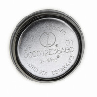
IBUTTON TEMP LOGGER
Manufacturer
Maxim Integrated Products
Series
iButton®r
Datasheet
1.DS1922L-F5.pdf
(52 pages)
Specifications of DS1922T-F5#
Rohs Information
IButton RoHS Compliance Plan
Memory Size
512B
Memory Type
NVSRAM (Non-Volatile SRAM)
Lead Free Status / RoHS Status
Lead free / RoHS Compliant
Temperature Logger iButton with 8KB
Data-Log Memory
The last step to begin a mission is to issue the Start
Mission command. As soon as they have received this
command, the DS1922L/DS1922T set the MIP flag and
clear the MEMCLR flag. With the immediate/delayed
start mode (SUTA = 0), and after as many minutes as
specified by the Mission Start Delay are over, the
device wakes up, copies the current date and time to
the Mission Timestamp register, and logs the first entry
of the mission. This increments both the Mission
Samples Counter and Device Samples Counter. All
subsequent log entries are made as specified by the
value in the Sample Rate register and the EHSS bit.
If the start upon temperature alarm mode is chosen
(SUTA = 1) and temperature logging is enabled (ETL =
1), the DS1922L/DS1922T first wait until the start delay
is over. Then the device wakes up in intervals as speci-
fied by the sample rate and EHSS bit and measures the
temperature. This increments the Device Samples
Counter register only. The first sample of the mission is
logged when the temperature alarm occurred.
However, the Mission Samples Counter does not incre-
ment. One sample period later the Mission Timestamp
register is set. From then on, both the Mission Samples
Counter and Device Samples Counter registers incre-
ment at the same time. All subsequent log entries are
made as specified by the value in the Sample Rate reg-
ister and the EHSS bit.
The general-purpose memory operates independently
of the other memory sections and is not write protected
during a mission. All the DS1922L/DS1922T’s memory
Figure 8. Address Registers
28
______________________________________________________________________________________
TARGET ADDRESS (TA1)
TARGET ADDRESS (TA2)
ENDING ADDRESS WITH
DATA STATUS (E/S)
BIT NUMBER
(READ ONLY)
T15
AA
T7
7
T14
T6
6
0
T13
T5
PF
5
can be read at any time, e.g., to watch the progress of
a mission. Attempts to read the passwords read 00h
bytes instead of the data that is stored in the password
registers.
Because of the serial data transfer, the DS1922L/
DS1922T employ three address registers called TA1,
TA2, and E/S (Figure 8). Registers TA1 and TA2 must
be loaded with the target address to which the data is
written or from which data is sent to the master upon a
Read command. Register E/S acts like a byte counter
and Transfer Status register. It is used to verify data
integrity with Write commands. Therefore, the master
only has read access to this register. The lower 5 bits of
the E/S register indicate the address of the last byte
that has been written to the scratchpad. This address is
called ending offset. The DS1922L/DS1922T require
that the ending offset is always 1Fh for a Copy
Scratchpad command to function. Bit 5 of the E/S
register, called PF or partial byte flag, is set if the num-
ber of data bits sent by the master is not an integer
multiple of 8. Bit 6 is always a 0. Note that the lowest 5
bits of the target address also determine the address
within the scratchpad, where intermediate storage of
data begins. This address is called byte offset. If the
target address for a Write command is 13Ch, for exam-
ple, the scratchpad stores incoming data beginning at
the byte offset 1Ch and is full after only 4 bytes. The
T12
T4
E4
4
Address Registers and Transfer Status
T11
T3
E3
3
T10
T2
E2
2
E1
T1
T9
1
Memory Access
E0
T0
T8
0


