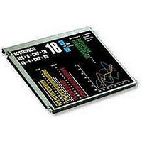
T-51511D150-FW-A-AC Optrex America Inc, T-51511D150-FW-A-AC Datasheet - Page 17

T-51511D150-FW-A-AC
Manufacturer Part Number
T-51511D150-FW-A-AC
Description
LCD 15.0" TFT MOD 1024X768 XGA
Manufacturer
Optrex America Inc
Datasheet
1.T-51511D150-FW-A-AC.pdf
(19 pages)
Specifications of T-51511D150-FW-A-AC
Display Type
TFT- Thin Film Transistor
Display Mode
Transmissive
Viewing Area
304.10mm L x 228.10mm W
Dot Pitch
0.30mm x 0.30mm
Dot Pixels
1024 x 768 (XGA)
Interface
TTL
Pixel Density
1024 x 768
Module Size (w X H X T)
326 mm x 255 mm x 15.5 mm
Backlighting
CCFL White
Lead Free Status / RoHS Status
Lead free / RoHS Compliant
Backlight
-
Dot Size
-
Lead Free Status / Rohs Status
No
Other names
73-1230
11. HANDLING PRECAUTIONS FOR TFT-LCD MODULE
Please pay attention to the followings in handling TFT-LCD products;
(1) ASSEMBLY PRECAUTION
a. Please mount the LCD module by using mounting hole with a screw clamping torque less than 0.5
b. Please design display housing in accordance with the following guide lines.
c. Please do not push or scratch LCD panel surface with anything hard. And do not soil LCD panel
d. Please do not press any parts on the rear side such as source TCP, gate TCP, control circuit board
e. Please wipe off LCD panel surface with absorbent cotton or soft cloth in case of it being soiled.
f. Please wipe off drops of adhesives like saliva and water on LCD panel surface immediately. They
g. Please do not take a LCD module to pieces and reconstruct it. Resolving and reconstructing modules
h. Please do not touch metal frames with bare hands and soiled gloves. A color change of the metal
i. Please pay attention to handling lead wire of backlight so that it is not tugged in connecting with
T-51511D150-FW-A-AC (AC) No. 2002-0229
Nm. Please do not bend or wrench the LCD module in assembling. Please do not drop, bend or twist
the LCD module in handling. Please mount the invertor circuit board by using mounting hole of
rear side with a screw clamping torque less than 0.2 Nm.
(a) Housing case must be designed carefully so as not to put stresses on LCD all sides and not to
(b) Keep sufficient clearance between LCD module back surface and housing when the LCD
(c) When some parts, such as, FPC cable and ferrite plate, are installed underneath the LCD
(d) Design the inverter location and connector position carefully so as not to give stress to lamp
(e) Keep sufficient clearance between LCD module and the others parts, such as inverter and
surface by touching with bare hands. (Polarizer film, surface of LCD panel is easy to be flawed.)
and FPCs during handling LCD module. If pressing rear part is unavoidable, handle the LCD
module with care not to damage them.
might damage to cause panel surface variation and color change.
may cause them not to work well.
frames can happen during a long preservation of soiled LCD modules.
inverter.
wrench module. The stresses may cause non-uniformity even if there is no non-uniformity
statically.
module is mounted. Approximately 1.0mm of the clearance in the design is recommended taking
into account the tolerance of LCD module thickness and mounting structure height on the
housing.
module, still sufficient clearance is required, such as 0.5mm. This clearance is, especially, to be
reconsidered when the additional parts are implemented for EMI countermeasure.
cable, or not to interface the LCD module by the lamp cable.
speaker so as not to interface the LCD module. Approximately 1.0mm of the clearance in the
design is recommended.
OPTREX CORPORATION
Page 18/33


