Z8F64220100ZDA Zilog, Z8F64220100ZDA Datasheet - Page 141
Z8F64220100ZDA
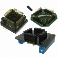
Manufacturer Part Number
Z8F64220100ZDA
Description
ADAPTER ICE Z8 ENCORE 64K 64LQFP
Manufacturer
Zilog
Specifications of Z8F64220100ZDA
Module/board Type
*
For Use With/related Products
Z8 Encore!™
Lead Free Status / RoHS Status
Contains lead / RoHS non-compliant
Other names
269-3403


PS019921-0308
SPI Signals
During an SPI transfer, data is sent and received simultaneously by both the Master and
the Slave SPI devices. Separate signals are required for data and the serial clock. When an
SPI transfer occurs, a multi-bit (typically 8-bit) character is shifted out one data pin and an
multi-bit character is simultaneously shifted in on a second data pin. An 8-bit shift register
in the Master and another 8-bit shift register in the Slave are connected as a circular buffer.
The SPI shift register is single-buffered in the transmit and receive directions. New data to
be transmitted cannot be written into the shift register until the previous transmission is
complete and receive data (if valid) has been read.
The four basic SPI signals are:
•
•
•
•
Each signal is described in both Master and Slave modes.
Master-In/Slave-Out
The Master-In/Slave-Out (MISO) pin is configured as an input in a Master device and as
an output in a Slave device. It is one of the two lines that transfer serial data, with the most
significant bit sent first. The MISO pin of a Slave device is placed in a high-impedance
state if the Slave is not selected. When the SPI is not enabled, this signal is in a high-
impedance state.
Master-Out/Slave-In
The Master-Out/Slave-In (MOSI) pin is configured as an output in a Master device and as
an input in a Slave device. It is one of the two lines that transfer serial data, with the most
significant bit sent first. When the SPI is not enabled, this signal is in a high-impedance
state.
Serial Clock
The Serial Clock (SCK) synchronizes data movement both in and out of the device
through its MOSI and MISO pins. In MASTER mode, the SPI’s Baud Rate Generator cre-
ates the serial clock. The Master drives the serial clock out its own SCK pin to the Slave’s
SCK pin. When the SPI is configured as a Slave, the SCK pin is an input and the clock sig-
nal from the Master synchronizes the data transfer between the Master and Slave devices.
Slave devices ignore the SCK signal, unless the SS pin is asserted. When configured as a
slave, the SPI block requires a minimum SCK period of greater than or equal to 8 times
the system (XIN) clock period.
Master-In/Slave-Out
Master-Out/Slave-In
Serial Clock
Slave Select
Z8 Encore! XP
Product Specification
Serial Peripheral Interface
®
F64XX Series
127
Related parts for Z8F64220100ZDA
Image
Part Number
Description
Manufacturer
Datasheet
Request
R

Part Number:
Description:
Communication Controllers, ZILOG INTELLIGENT PERIPHERAL CONTROLLER (ZIP)
Manufacturer:
Zilog, Inc.
Datasheet:

Part Number:
Description:
KIT DEV FOR Z8 ENCORE 16K TO 64K
Manufacturer:
Zilog
Datasheet:

Part Number:
Description:
KIT DEV Z8 ENCORE XP 28-PIN
Manufacturer:
Zilog
Datasheet:

Part Number:
Description:
DEV KIT FOR Z8 ENCORE 8K/4K
Manufacturer:
Zilog
Datasheet:

Part Number:
Description:
KIT DEV Z8 ENCORE XP 28-PIN
Manufacturer:
Zilog
Datasheet:

Part Number:
Description:
DEV KIT FOR Z8 ENCORE 4K TO 8K
Manufacturer:
Zilog
Datasheet:
Part Number:
Description:
CMOS Z8 microcontroller. ROM 16 Kbytes, RAM 256 bytes, speed 16 MHz, 32 lines I/O, 3.0V to 5.5V
Manufacturer:
Zilog, Inc.
Datasheet:
Part Number:
Description:
Low-cost microcontroller. 512 bytes ROM, 61 bytes RAM, 8 MHz
Manufacturer:
Zilog, Inc.
Datasheet:
Part Number:
Description:
Z8 4K OTP Microcontroller
Manufacturer:
Zilog, Inc.
Datasheet:
Part Number:
Description:
CMOS SUPER8 ROMLESS MCU
Manufacturer:
Zilog, Inc.
Datasheet:
Part Number:
Description:
SL1866 CMOSZ8 OTP Microcontroller
Manufacturer:
Zilog, Inc.
Datasheet:
Part Number:
Description:
SL1866 CMOSZ8 OTP Microcontroller
Manufacturer:
Zilog, Inc.
Datasheet:
Part Number:
Description:
OTP (KB) = 1, RAM = 125, Speed = 12, I/O = 14, 8-bit Timers = 2, Comm Interfaces Other Features = Por, LV Protect, Voltage = 4.5-5.5V
Manufacturer:
Zilog, Inc.
Datasheet:
Part Number:
Description:
Manufacturer:
Zilog, Inc.
Datasheet: