OM6290 NXP Semiconductors, OM6290 Datasheet - Page 6
OM6290
Manufacturer Part Number
OM6290
Description
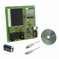
DEMO BOARD LCD GRAPHIC DRIVER
Manufacturer
NXP Semiconductors
Datasheets
1.PCF8576T1118.pdf
(44 pages)
2.OM6290.pdf
(30 pages)
3.OM6290.pdf
(51 pages)
4.OM6290.pdf
(83 pages)
Specifications of OM6290
Main Purpose
Displays, LCD Controller
Embedded
Yes, MCU, 16/32-Bit
Utilized Ic / Part
PCF2119, PCF8531, PCF8576
Primary Attributes
Character, Graphic and Segment LCD Drivers
Secondary Attributes
JTAG, I²C, UART & USB Interfaces
Description/function
Demo Board
Interface Type
USB, I2C, JTAG, UART
Data Bus Width
4 bit, 8 bit, 16 bit
Operating Voltage
1.8 V to 5.5 V
For Use With/related Products
PCF8576DT, PCF2119S, PCF8531
Lead Free Status / RoHS Status
Lead free / RoHS Compliant
Lead Free Status / RoHS Status
Lead free / RoHS Compliant, Lead free / RoHS Compliant
Other names
568-4703


NXP Semiconductors
UM10300_1
User manual
2.4 Connectors
2.5 Reserved components
On the left below LCD3 a pin strip P3 is available which carries the following signals: 5V,
3V3, SCL, GND, SDA and nRES. The latter is connected to the reset circuit IC6 and by
making nRES LOW, a defined reset signal is generated.
On the right side of the board a USB connector has been provided. At the time of writing
the first revision of this manual the only purpose of the USB connector is to offer the
option of powering the board via USB. Future updates of the firmware which would also
enable data communication between the LCD driver ICs and a GUI which then would run
on a PC, are under consideration.
The serial interface RS1 (UART) below the USB connector is used for updating the
firmware in the microcontroller.
The board layout includes a few components which are not directly necessary for the
primary purpose of the board which is providing a hands-on tool to work with the three
different types of NXP LCD drivers. Therefore these components are not mounted.
However, in some scenario’s it may be desired to explore more of the options of the on-
board microcontroller. Therefore three optional areas may be mounted by the user of the
board in order to add extra functionality.
Besides these microcontroller related items, another option is to remove resistor R29
(470 Ω) and mount potentiometer Pot1 (4k7) instead. This enables adjustment of the
contrast of display LCD3. The location of these components is between LCD2 and LCD3.
1. Real Time Clock of LPC2148: By mounting a 32.768 kHz crystal at position Y2 as
2. JTAG interface: On the right side of the board under LCD1, space is provided for a
3. Pin strips P1 and P2 near the bottom edge of the board. If a pin strip is soldered on
well as two capacitors at positions C29, C30 the internal RTC can be used. The
values of C29 and C30 depend on the crystal used. A crystal for an RTC is designed
to operate with a certain load capacitance C
capacitance of such a crystal is 12.5 pF. Seen from the crystal C29 and C30 are in
series. Taking into account parasitic capacitances as well, C29 and C30 will have to
be 22 pF or 25 pF if a 12.5 pF crystal is used.
JTAG connector. This is a 20-pin header with pitch of 2.54 mm. The required pull-up
resistors are already mounted.
the board at this position, all unused pins of the microcontroller are accessible.
If mounted, exercise caution not to overload these signal lines !
Rev. 1.0— 8 August 2008
L
. A common value for the required load
User Manual OM6290
UM10300
© NXP B.V. 2008. All rights reserved.
6 of 30
Related parts for OM6290
Image
Part Number
Description
Manufacturer
Datasheet
Request
R

Part Number:
Description:
NXP Semiconductors designed the LPC2420/2460 microcontroller around a 16-bit/32-bitARM7TDMI-S CPU core with real-time debug interfaces that include both JTAG andembedded trace
Manufacturer:
NXP Semiconductors
Datasheet:

Part Number:
Description:
NXP Semiconductors designed the LPC2458 microcontroller around a 16-bit/32-bitARM7TDMI-S CPU core with real-time debug interfaces that include both JTAG andembedded trace
Manufacturer:
NXP Semiconductors
Datasheet:
Part Number:
Description:
NXP Semiconductors designed the LPC2468 microcontroller around a 16-bit/32-bitARM7TDMI-S CPU core with real-time debug interfaces that include both JTAG andembedded trace
Manufacturer:
NXP Semiconductors
Datasheet:
Part Number:
Description:
NXP Semiconductors designed the LPC2470 microcontroller, powered by theARM7TDMI-S core, to be a highly integrated microcontroller for a wide range ofapplications that require advanced communications and high quality graphic displays
Manufacturer:
NXP Semiconductors
Datasheet:
Part Number:
Description:
NXP Semiconductors designed the LPC2478 microcontroller, powered by theARM7TDMI-S core, to be a highly integrated microcontroller for a wide range ofapplications that require advanced communications and high quality graphic displays
Manufacturer:
NXP Semiconductors
Datasheet:
Part Number:
Description:
The Philips Semiconductors XA (eXtended Architecture) family of 16-bit single-chip microcontrollers is powerful enough to easily handle the requirements of high performance embedded applications, yet inexpensive enough to compete in the market for hi
Manufacturer:
NXP Semiconductors
Datasheet:
Part Number:
Description:
The XA-S3 device is a member of Philips Semiconductors? XA(eXtended Architecture) family of high performance 16-bitsingle-chip microcontrollers
Manufacturer:
NXP Semiconductors
Datasheet:

Part Number:
Description:
The NXP BlueStreak LH75401/LH75411 family consists of two low-cost 16/32-bit System-on-Chip (SoC) devices
Manufacturer:
NXP Semiconductors
Datasheet:
Part Number:
Description:
The NXP LPC3130/3131 combine an 180 MHz ARM926EJ-S CPU core, high-speed USB2
Manufacturer:
NXP Semiconductors
Datasheet:
Part Number:
Description:
The NXP LPC3141 combine a 270 MHz ARM926EJ-S CPU core, High-speed USB 2
Manufacturer:
NXP Semiconductors
Part Number:
Description:
The NXP LPC3143 combine a 270 MHz ARM926EJ-S CPU core, High-speed USB 2
Manufacturer:
NXP Semiconductors

Part Number:
Description:
The NXP LPC3152 combines an 180 MHz ARM926EJ-S CPU core, High-speed USB 2
Manufacturer:
NXP Semiconductors
Part Number:
Description:
The NXP LPC3154 combines an 180 MHz ARM926EJ-S CPU core, High-speed USB 2
Manufacturer:
NXP Semiconductors

Part Number:
Description:
Standard level N-channel enhancement mode Field-Effect Transistor (FET) in a plastic package using NXP High-Performance Automotive (HPA) TrenchMOS technology
Manufacturer:
NXP Semiconductors
Datasheet: