OM6290 NXP Semiconductors, OM6290 Datasheet - Page 25
OM6290
Manufacturer Part Number
OM6290
Description
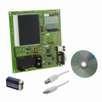
DEMO BOARD LCD GRAPHIC DRIVER
Manufacturer
NXP Semiconductors
Datasheets
1.PCF8576T1118.pdf
(44 pages)
2.OM6290.pdf
(30 pages)
3.OM6290.pdf
(51 pages)
4.OM6290.pdf
(83 pages)
Specifications of OM6290
Main Purpose
Displays, LCD Controller
Embedded
Yes, MCU, 16/32-Bit
Utilized Ic / Part
PCF2119, PCF8531, PCF8576
Primary Attributes
Character, Graphic and Segment LCD Drivers
Secondary Attributes
JTAG, I²C, UART & USB Interfaces
Description/function
Demo Board
Interface Type
USB, I2C, JTAG, UART
Data Bus Width
4 bit, 8 bit, 16 bit
Operating Voltage
1.8 V to 5.5 V
For Use With/related Products
PCF8576DT, PCF2119S, PCF8531
Lead Free Status / RoHS Status
Lead free / RoHS Compliant
Lead Free Status / RoHS Status
Lead free / RoHS Compliant, Lead free / RoHS Compliant
Other names
568-4703


NXP Semiconductors
PCF2119X
Product data sheet
Fig 16. Relationship between CGRAM addresses, data and display patterns
7
0
0
0
0
0
0
0
(1) Character code bit 0 to bit 3 correspond to CGRAM address bit 3 to bit 6.
(2) CGRAM address bit 0 to bit 2 designate the character pattern line position. The 8th line is the cursor position and display is
(3) Character pattern column positions correspond to CGRAM data bit 0 to bit 4, as shown in
(4) As shown in
(5) Only bit 0 to bit 5 of the CGRAM address are set by the Set_CGRAM command. Bit 6 can be set using the Set_DDRAM
higher
order
6
bits
0
0
0
0
0
0
0
(4)
character codes
performed by logical OR with the cursor. Data in the 8th line will appear in the cursor position. Lines are numbered from 0 to 7.
CGRAM data = logic 1 corresponds to selection for display.
command in the valid address range or by using the auto-increment feature during CGRAM write. All bits from bit 0 to bit 6 can
be read using the BF_AC instruction.
(DDRAM data)
5
0
0
0
0
0
0
0
4
0
0
0
0
0
0
0
3
0
0
0
1
1
1
1
9.3 CGRAM
2
0
0
0
1
1
1
1
Figure 10
lower
(1)
order
bits
1
0
0
1
1
1
1
1
Up to 16 user defined characters may be stored in the Character Generator RAM
(CGRAM). Some CGRAM characters (see
When the icons blink option is enabled, double the number of CGRAM characters are
used since both the on and off state of an icon is defined.
The CGROM and CGRAM use a common address space, of which the first column is
reserved for the CGRAM (see
Figure 16
•
•
•
0
0
1
0
1
1
1
1
6 CGRAM characters if icons blink and both icon rows are used in the application
3 CGRAM characters if no icons blink but both icon rows are used in the application
0 CGRAM characters if no icons are driven by the icon rows
to
Figure
1
1
1
1
0
6
0
0
shows the addressing principle for the CGRAM.
higher
order
bits
0
0
0
1
1
1
1
5
(1)
15, CGRAM character patterns are selected when character code bit 4 to bit 7 are all logic 0.
(5)
1
1
1
1
0
0
1
4
CGRAM
address
All information provided in this document is subject to legal disclaimers.
(2)
3
0
1
0
1
1
1
1
0
0
0
0
1
1
1
1
0
0
0
0
1
1
1
1
0
0
1
1
1
1
2
lower
order
bits
0
0
1
1
0
0
1
1
0
0
1
1
0
0
1
1
0
0
0
0
1
1
1
Rev. 9 — 14 April 2011
0
0
1
0
1
0
1
0
1
0
1
0
1
0
1
0
1
0
1
0
1
0
1
Figure 10
higher
order
bits
4
0
0
0
0
0
0
to
character patterns
(CGRAM data)
Figure
Figure
3
0
0
0
0
0
0
0
0
0
0
0
2
0
0
0
0
0
0
0
0
lower
order
bits
1
0
0
0
0
0
0
0
0
0
0
22) are also used to drive icons:
15).
0
0
0
0
0
0
0
0
0
0
0
example 1
example 2
character
character
pattern
position
pattern
cursor
Figure 10
LCD controllers/drivers
to
PCF2119x
Figure
4
1
1
1
1
1
1
1
0
1
0
1
0
1
0
0
0
© NXP B.V. 2011. All rights reserved.
character code
(CGRAM data)
3
1
0
0
1
0
0
0
0
0
1
1
0
1
0
0
0
15.
2
1
0
0
1
1
0
0
0
0
0
1
1
1
1
1
0
1
1
0
0
1
0
1
0
0
0
1
1
0
1
0
0
0
coa072
0
0
1
1
0
0
0
1
0
1
0
1
0
1
0
0
0
25 of 83
(3)
Related parts for OM6290
Image
Part Number
Description
Manufacturer
Datasheet
Request
R

Part Number:
Description:
NXP Semiconductors designed the LPC2420/2460 microcontroller around a 16-bit/32-bitARM7TDMI-S CPU core with real-time debug interfaces that include both JTAG andembedded trace
Manufacturer:
NXP Semiconductors
Datasheet:

Part Number:
Description:
NXP Semiconductors designed the LPC2458 microcontroller around a 16-bit/32-bitARM7TDMI-S CPU core with real-time debug interfaces that include both JTAG andembedded trace
Manufacturer:
NXP Semiconductors
Datasheet:
Part Number:
Description:
NXP Semiconductors designed the LPC2468 microcontroller around a 16-bit/32-bitARM7TDMI-S CPU core with real-time debug interfaces that include both JTAG andembedded trace
Manufacturer:
NXP Semiconductors
Datasheet:
Part Number:
Description:
NXP Semiconductors designed the LPC2470 microcontroller, powered by theARM7TDMI-S core, to be a highly integrated microcontroller for a wide range ofapplications that require advanced communications and high quality graphic displays
Manufacturer:
NXP Semiconductors
Datasheet:
Part Number:
Description:
NXP Semiconductors designed the LPC2478 microcontroller, powered by theARM7TDMI-S core, to be a highly integrated microcontroller for a wide range ofapplications that require advanced communications and high quality graphic displays
Manufacturer:
NXP Semiconductors
Datasheet:
Part Number:
Description:
The Philips Semiconductors XA (eXtended Architecture) family of 16-bit single-chip microcontrollers is powerful enough to easily handle the requirements of high performance embedded applications, yet inexpensive enough to compete in the market for hi
Manufacturer:
NXP Semiconductors
Datasheet:
Part Number:
Description:
The XA-S3 device is a member of Philips Semiconductors? XA(eXtended Architecture) family of high performance 16-bitsingle-chip microcontrollers
Manufacturer:
NXP Semiconductors
Datasheet:

Part Number:
Description:
The NXP BlueStreak LH75401/LH75411 family consists of two low-cost 16/32-bit System-on-Chip (SoC) devices
Manufacturer:
NXP Semiconductors
Datasheet:
Part Number:
Description:
The NXP LPC3130/3131 combine an 180 MHz ARM926EJ-S CPU core, high-speed USB2
Manufacturer:
NXP Semiconductors
Datasheet:
Part Number:
Description:
The NXP LPC3141 combine a 270 MHz ARM926EJ-S CPU core, High-speed USB 2
Manufacturer:
NXP Semiconductors
Part Number:
Description:
The NXP LPC3143 combine a 270 MHz ARM926EJ-S CPU core, High-speed USB 2
Manufacturer:
NXP Semiconductors

Part Number:
Description:
The NXP LPC3152 combines an 180 MHz ARM926EJ-S CPU core, High-speed USB 2
Manufacturer:
NXP Semiconductors
Part Number:
Description:
The NXP LPC3154 combines an 180 MHz ARM926EJ-S CPU core, High-speed USB 2
Manufacturer:
NXP Semiconductors

Part Number:
Description:
Standard level N-channel enhancement mode Field-Effect Transistor (FET) in a plastic package using NXP High-Performance Automotive (HPA) TrenchMOS technology
Manufacturer:
NXP Semiconductors
Datasheet: