OM6290 NXP Semiconductors, OM6290 Datasheet - Page 14
OM6290
Manufacturer Part Number
OM6290
Description
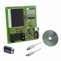
DEMO BOARD LCD GRAPHIC DRIVER
Manufacturer
NXP Semiconductors
Datasheets
1.PCF8576T1118.pdf
(44 pages)
2.OM6290.pdf
(30 pages)
3.OM6290.pdf
(51 pages)
4.OM6290.pdf
(83 pages)
Specifications of OM6290
Main Purpose
Displays, LCD Controller
Embedded
Yes, MCU, 16/32-Bit
Utilized Ic / Part
PCF2119, PCF8531, PCF8576
Primary Attributes
Character, Graphic and Segment LCD Drivers
Secondary Attributes
JTAG, I²C, UART & USB Interfaces
Description/function
Demo Board
Interface Type
USB, I2C, JTAG, UART
Data Bus Width
4 bit, 8 bit, 16 bit
Operating Voltage
1.8 V to 5.5 V
For Use With/related Products
PCF8576DT, PCF2119S, PCF8531
Lead Free Status / RoHS Status
Lead free / RoHS Compliant
Lead Free Status / RoHS Status
Lead free / RoHS Compliant, Lead free / RoHS Compliant
Other names
568-4703


Philips Semiconductors
6.5
6.5.1
The internal logic and the LCD drive signals of the
PCF8576 are timed either by the internal oscillator or from
an external clock. When the internal oscillator is used,
pin OSC should be connected to pin V
output from pin CLK provides the clock signal for
cascaded PCF8566s in the system.
Where resistor R
is selected. The relationship between the oscillator
frequency on pin CLK (f
6.5.2
The condition for external clock is made by connecting
pin OSC to pin V
clock input.
The clock frequency (f
frequency and the maximum rate for data reception from
the I
maximum data rate of 100 kHz, f
above 125 kHz.
A clock signal must always be supplied to the device;
removing the clock may freeze the LCD in a DC state.
2001 Oct 02
Universal LCD driver for low multiplex rates
2
f
Fig.9 Oscillator frequency as a function of R
clk
C-bus. To allow I
(kHz)
10
f
10
clk
Oscillator
10
3
2
I
10
E
3.4 10
----------------------- - kHz
NTERNAL CLOCK
XTERNAL CLOCK
2
R
osc
7
osc
DD
; pin CLK then becomes the external
to V
min
clk
2
max
C-bus transmissions at their
SS
clk
) determines the LCD frame
) and R
is present, the internal oscillator
10
3
clk
osc
should be chosen to be
R
is shown in Fig.9.
osc
SS
(k
. In this event, the
MBE531
10
4
osc
.
14
6.6
The timing of the PCF8576 organizes the internal data flow
of the device. This includes the transfer of display data
from the display RAM to the display segment outputs. In
cascaded applications, the synchronization signal SYNC
maintains the correct timing relationship between the
PCF8576s in the system. The timing also generates the
LCD frame frequency which it derives as an integer
multiple of the clock frequency (see Table 2). The frame
frequency is set by the MODE SET commands when
internal clock is used, or by the frequency applied to
pin CLK when external clock is used.
The ratio between the clock frequency and the LCD frame
frequency depends on the mode in which the device is
operating. In the power-saving mode the reduction ratio is
six times smaller; this allows the clock frequency to be
reduced by a factor of six. The reduced clock frequency
results in a significant reduction in power dissipation. The
lower clock frequency has the disadvantage of increasing
the response time when large amounts of display data are
transmitted on the I
When a device is unable to digest a display data byte
before the next one arrives, it holds the SCL line LOW until
the first display data byte is stored. This slows down the
transmission rate of the I
Table 2 LCD frame frequencies
6.7
The display latch holds the display data while the
corresponding multiplex signals are generated. There is a
one-to-one relationship between the data in the display
latch, the LCD segment outputs and one column of the
display RAM.
6.8
The shift register serves to transfer display information
from the display RAM to the display latch while previous
data is displayed.
Normal mode
Power-saving mode
PCF8576 MODE
Timing
Display latch
Shift register
2
C-bus.
FREQUENCY
2
C-bus but no data loss occurs.
FRAME
------------ -
2880
--------- -
480
f
f
clk
clk
Product specification
PCF8576
FREQUENCY
NOMINAL
FRAME
(Hz)
64
64
Related parts for OM6290
Image
Part Number
Description
Manufacturer
Datasheet
Request
R

Part Number:
Description:
NXP Semiconductors designed the LPC2420/2460 microcontroller around a 16-bit/32-bitARM7TDMI-S CPU core with real-time debug interfaces that include both JTAG andembedded trace
Manufacturer:
NXP Semiconductors
Datasheet:

Part Number:
Description:
NXP Semiconductors designed the LPC2458 microcontroller around a 16-bit/32-bitARM7TDMI-S CPU core with real-time debug interfaces that include both JTAG andembedded trace
Manufacturer:
NXP Semiconductors
Datasheet:
Part Number:
Description:
NXP Semiconductors designed the LPC2468 microcontroller around a 16-bit/32-bitARM7TDMI-S CPU core with real-time debug interfaces that include both JTAG andembedded trace
Manufacturer:
NXP Semiconductors
Datasheet:
Part Number:
Description:
NXP Semiconductors designed the LPC2470 microcontroller, powered by theARM7TDMI-S core, to be a highly integrated microcontroller for a wide range ofapplications that require advanced communications and high quality graphic displays
Manufacturer:
NXP Semiconductors
Datasheet:
Part Number:
Description:
NXP Semiconductors designed the LPC2478 microcontroller, powered by theARM7TDMI-S core, to be a highly integrated microcontroller for a wide range ofapplications that require advanced communications and high quality graphic displays
Manufacturer:
NXP Semiconductors
Datasheet:
Part Number:
Description:
The Philips Semiconductors XA (eXtended Architecture) family of 16-bit single-chip microcontrollers is powerful enough to easily handle the requirements of high performance embedded applications, yet inexpensive enough to compete in the market for hi
Manufacturer:
NXP Semiconductors
Datasheet:
Part Number:
Description:
The XA-S3 device is a member of Philips Semiconductors? XA(eXtended Architecture) family of high performance 16-bitsingle-chip microcontrollers
Manufacturer:
NXP Semiconductors
Datasheet:

Part Number:
Description:
The NXP BlueStreak LH75401/LH75411 family consists of two low-cost 16/32-bit System-on-Chip (SoC) devices
Manufacturer:
NXP Semiconductors
Datasheet:
Part Number:
Description:
The NXP LPC3130/3131 combine an 180 MHz ARM926EJ-S CPU core, high-speed USB2
Manufacturer:
NXP Semiconductors
Datasheet:
Part Number:
Description:
The NXP LPC3141 combine a 270 MHz ARM926EJ-S CPU core, High-speed USB 2
Manufacturer:
NXP Semiconductors
Part Number:
Description:
The NXP LPC3143 combine a 270 MHz ARM926EJ-S CPU core, High-speed USB 2
Manufacturer:
NXP Semiconductors

Part Number:
Description:
The NXP LPC3152 combines an 180 MHz ARM926EJ-S CPU core, High-speed USB 2
Manufacturer:
NXP Semiconductors
Part Number:
Description:
The NXP LPC3154 combines an 180 MHz ARM926EJ-S CPU core, High-speed USB 2
Manufacturer:
NXP Semiconductors

Part Number:
Description:
Standard level N-channel enhancement mode Field-Effect Transistor (FET) in a plastic package using NXP High-Performance Automotive (HPA) TrenchMOS technology
Manufacturer:
NXP Semiconductors
Datasheet: