EVAL-ADF4252EBZ2 Analog Devices Inc, EVAL-ADF4252EBZ2 Datasheet - Page 5
EVAL-ADF4252EBZ2
Manufacturer Part Number
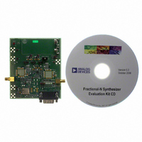
EVAL-ADF4252EBZ2
Description
BOARD EVAL ADF4252 NO VCO/FILTER
Manufacturer
Analog Devices Inc
Datasheet
1.ADF4252BCPZ.pdf
(28 pages)
Specifications of EVAL-ADF4252EBZ2
Main Purpose
Timing, Frequency Synthesizer
Embedded
No
Utilized Ic / Part
ADF4252
Primary Attributes
Dual Fractional-N PLL
Secondary Attributes
Board excludes Loop Filter & VCO
Lead Free Status / RoHS Status
Lead free / RoHS Compliant


Mnemonic
CP
CP
RF
RF
A
MUXOUT
REF
REF
D
CLK
DATA
LE
R
A
IF
IF
DV
CP
CP
V
V
V
V
V
REV. B
GND
SET
GND
P
DD
DD
DD
P
GND
IN
IN
2
1
RF
GND
IN
IN
GND
IF
DD
B
A
2
3
1
IN
OUT
A
B
1
2
1
2
This multiplexer output allows either the RF or IF lock detect, the scaled RF or IF, or the scaled reference fre-
Serial Data Input. The serial data is loaded MSB first with the three LSBs being the control bits. This input is a
Function
RF Charge Pump Output. This is normally connected to a loop filter that drives the input to an external VCO.
RF Charge Pump Ground.
Input to the RF Prescaler. This small signal input is normally taken from the VCO.
Complementary Input to the RF Prescaler.
Analog Ground for the RF Synthesizer.
quency to be accessed externally.
Reference Input. This is a CMOS input with a nominal threshold of V
100 kΩ. This input can be driven from a TTL or CMOS crystal oscillator.
Reference Output.
Digital Ground for the Fractional Interpolator.
Serial Clock Input. This serial clock is used to clock in the serial data to the registers. The data is latched into the
shift register on the CLK rising edge. This input is a high impedance CMOS input.
high impedance CMOS input.
Load Enable, CMOS Input. When LE goes high, the data stored in the shift registers is loaded into one of the
seven latches, the latch being selected using the control bits.
Connecting a resistor between this pin and ground sets the minimum charge pump output current. The relationship
between I
Therefore, with R
Ground for the IF Synthesizer.
Complementary Input to the IF Prescaler.
Input to the IF Prescaler. This small signal input is normally taken from the IF VCO.
Positive Power Supply for the Fractional Interpolator Section. Decoupling capacitors to the ground plane should
be placed as close as possible to this pin. DV
IF Charge Pump Ground.
IF Charge Pump Output. This is normally connected to a loop filter that drives the input to an external VCO.
IF Charge Pump Power Supply. Decoupling capacitors to the ground plane should be placed as close as possible
to this pin. This voltage should be greater than or equal to V
Positive Power Supply for the IF Section. Decoupling capacitors to the ground plane should be placed as close as
possible to this pin. V
Positive Power Supply for the RF Digital Section. Decoupling capacitors to the ground plane should be placed as close
as possible to this pin. V
Positive Power Supply for the RF Analog Section. Decoupling capacitors to the ground plane should be placed as close
as possible to this pin. V
RF Charge Pump Power Supply. Decoupling capacitors to the ground plane should be placed as close as possible
to this pin. This voltage should be greater than or equal to V
I
CP
min
=
1 6875
CP
R
.
SET
and R
SET
SET
= 2.7 kΩ, I
DD
is
DD
DD
2 has a value 3 V ± 10%. V
3 has a value 3 V ± 10%. V
1 has a value 3 V ± 10%. V
PIN FUNCTION DESCRIPTIONS
CPmin
= 0.625 mA.
DD
–5–
must have the same voltage as V
DD
DD
DD
2 must have the same voltage as V
3 must have the same voltage as V
1 must have the same voltage as V
DD
DD
2.
1.
DD
/2 and an equivalent input resistance of
DD
1, V
DD
DD
DD
DD
2, and V
1, V
2, V
1, V
DD
DD
DD
ADF4252
2, and DV
3, and DV
3, and DV
DD
3.
DD
DD
DD
.
.
.
Related parts for EVAL-ADF4252EBZ2
Image
Part Number
Description
Manufacturer
Datasheet
Request
R

Part Number:
Description:
IC, ADJ LDO REG, 1.5V TO 5V 250mA MSOP-8
Manufacturer:
Vishay
Datasheet:

Part Number:
Description:
IC, ADJ LDO REG, 1.5V TO 5V 0.6A 8-TSSOP
Manufacturer:
Vishay
Datasheet:
Part Number:
Description:
IC, ADJ LDO REG, 1.5V TO 5V 250mA MSOP-8
Manufacturer:
Vishay
Datasheet:

Part Number:
Description:
IC ADJ LDO REG 1.5V TO 5V 150mA 5-SOT-23
Manufacturer:
Vishay
Datasheet:

Part Number:
Description:
BOARD EVAL AS1324-AD
Manufacturer:
austriamicrosystems
Datasheet:
Part Number:
Description:
IC, ADJ LDO REG, 1.5V TO 5V 0.6A 8-TSSOP
Manufacturer:
Vishay
Datasheet:

Part Number:
Description:
IC, ADJ LDO REG, 1.5V TO 5V, 0.3A, MSOP8
Manufacturer:
Vishay
Datasheet:
Part Number:
Description:
IC, ADJ LDO REG, 1.5V TO 5V, 0.3A, MSOP8
Manufacturer:
Vishay
Datasheet:
Part Number:
Description:
IC, ADJ LDO REG 1.215V TO 5V 0.3A MSOP-8
Manufacturer:
Vishay
Datasheet:
Part Number:
Description:
IC, ADJ LDO REG 1.215V TO 5V 0.3A MSOP-8
Manufacturer:
Vishay
Datasheet:

Part Number:
Description:
±1.7g Dual-Axis IMEMS Accelerometer Evaluation Board
Manufacturer:
Analog Devices Inc
Datasheet:

Part Number:
Description:
IC MULTIPLIER ANALOG 8-SOIC T/R
Manufacturer:
Analog Devices Inc
Datasheet:

Part Number:
Description:
IC ANALOG MULTIPLIER 8-DIP
Manufacturer:
Analog Devices Inc
Datasheet:
Part Number:
Description:
IC ANALOG MULTIPLIER 8-SOIC
Manufacturer:
Analog Devices Inc
Datasheet:
Part Number:
Description:
IC ANALOG MULTIPLIER 8-DIP
Manufacturer:
Analog Devices Inc
Datasheet: