W682510DK Nuvoton Technology Corporation of America, W682510DK Datasheet
W682510DK
Specifications of W682510DK


Related parts for W682510DK

W682510DK Summary of contents
Page 1
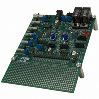
Winbond W682x10 Dual Channel CODEC Evaluation System User Guide W682x10DK Evaluation Board Winbond Electronics Corporation America 2727 N First Street, San Jose CA 95134 Rev 1.06 682x10DK 1 ...
Page 2
Overview ...................................................................................................... 3 1.1 Introduction ............................................................................................ 3 1.2 General Description ............................................................................... 3 1.3 W682x10DK Features............................................................................ 3 1.4 Reference Documents ........................................................................... 3 1.5 Pin name cross reference ...................................................................... 3 2 Hardware...................................................................................................... 4 2.1 CODEC block description ...................................................................... 4 2.2 Parallel ...
Page 3
Overview 1.1 Introduction The dual channel W682310 and W682510 (hereafter referred to as W682x10) are members of the W68XXXX family of PCM CODECs. The dual voice band CODEC complies with the ITU-T G.712 industry telecom specifications. The W682x10 also ...
Page 4
Hardware 2.1 CODEC block description The W682x10 CODEC is a dual channel CODEC that consists of two A/D converters (AI1-2) and two D/A converters (RO1-2) as shown below. RO1 (AOUT1) to Speaker MIC to AI1 (AIN1) RO2 (AOUT2) to ...
Page 5
To set up the handsets to communicate over parallel and serial mode, connect the digital channels as follows: Parallel mode (In same time slot) • Set SW7 to VCC position to set CHPS to VCC • Connect DIN1 to DOUT2 ...
Page 6
Default switch and jumper settings The default settings in the following table will enable operation of the board in parallel PCM mode, a-Law and two handsets communicating with each other using the on board clock generator 2.8.1 Signal Switches ...
Page 7
Location of switches, jumpers and connectors MIC 1 Polarity (SW12) Handset 1 (J2) Handset 2 (J3) EXT 5 VDC (J7) Power (SW11) 9 VDC (J5) u-Law PDN A-Law (SW6) (SW5) Winbond Electronics Corporation America 2727 N First Street, San ...
Page 8
Operating Modes The two handsets can be connected using either parallel or serial modes for simple verification of digital multiplexing modes. SW6 sets the mode and the jumper on J3 selects the digital signals to interconnect. 3.1 Two handsets ...
Page 9
Schematics 4.1 Clock and power circuits Y1 VCC VCC VCC GND OUT C12 2 TTL_OSC 2.048 MHz 0.1uF 0.1uF 13 12 74HC393/SO PWR: OFF - CASE SW11 ...
Page 10
CODEC and analog circuits VCC C3 0.1uF + C1 AOUT2 buffer: off - on C2 SW2 0.1uF 10uF tant@16v EG1903-ND AOUT2 LM358 C6 AOUT1 buffer: off - on U2A EG1903-ND 2 SW3 SPEAKER2 - 0.1uF R5 ...