STEVAL-CCH002V1 STMicroelectronics, STEVAL-CCH002V1 Datasheet - Page 36
STEVAL-CCH002V1
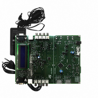
Manufacturer Part Number
STEVAL-CCH002V1
Description
BOARD EVAL HDMI $ VIDEO SWITCH
Manufacturer
STMicroelectronics
Specifications of STEVAL-CCH002V1
Design Resources
STEVAL-CCH002V1 Gerber Files STEVAL-CCH002V1 Schematic STEVAL-CCH002V1 Bill of Material
Main Purpose
Video, HDMI and Video Switches
Embedded
Yes, MCU, 8-Bit
Utilized Ic / Part
STMAV335, STMAV340, STHDMI002A, STDVE003A
Primary Attributes
DVI-I, 2 HDMI, Y Pb Pr, S-Video, CVBS, VGA - Input and Output
Secondary Attributes
LCD Displays Selection Status of Video Switches and Buffers
Lead Free Status / RoHS Status
Lead free / RoHS Compliant
Other names
497-8371


Application information
5
5.1
5.2
5.3
36/42
Application information
Power supply sequencing
Proper power-supply sequencing is advised for all CMOS devices. It is recommended to
always apply V
Power supply requirements
Bypass each of the V
device as possible, with the smaller-valued capacitor as close to the V
possible.
All V
from each V
variation can only be ±5% as per the HDMI specifications.
The maximum tolerable noise ripple on 3.3 V supply must be within a specified limit.
Differential traces
The high-speed TMDS inputs are the most critical parts for the device. There are several
considerations to minimize discontinuities on these transmission lines between the
connectors and the device.
(a) Maintain 100-Ω differential transmission line impedance into and out of the STDVE003A.
(b) Keep an uninterrupted ground plane below the high-speed I/Os.
(c) Keep the ground-path vias to the device as close as possible to allow the shortest return
current path.
(d) Layout of the TMDS differential inputs should be with the shortest stubs from the
connectors.
Output trace characteristics affect the performance of the STDVE003A. Use controlled
impedance traces to match trace impedance to both the transmission medium impedance
and termination resistor. Run the differential traces close together to minimize the effects of
the noise. Reduce skew by matching the electrical length of the traces. Avoid discontinuities
in the differential trace layout. Avoid 90 degree turns and minimize the number of vias to
further prevent impedance discontinuities.
CC
pins can be tied to a single 3.3 V power source. A 0.01 μF capacitor is connected
CC
CC
pin directly to ground to filter supply noise. The maximum power supply
before applying any signals to the input/output or control pins.
CC
pins with 0.1 μF and 1 nF capacitors in parallel as close to the
CC
pin of the device as
STDVE003A
Related parts for STEVAL-CCH002V1
Image
Part Number
Description
Manufacturer
Datasheet
Request
R

Part Number:
Description:
EVAL BOARD CC DRVR HI DENSE LEDS
Manufacturer:
STMicroelectronics
Datasheet:

Part Number:
Description:
EVAL BOARD CC DRVR HI DENSE LEDS
Manufacturer:
STMicroelectronics
Datasheet:

Part Number:
Description:
BATTERY CHARGER CELL PHONE
Manufacturer:
STMicroelectronics
Datasheet:

Part Number:
Description:
BOARD EVAL FOR MEMS SENSORS
Manufacturer:
STMicroelectronics
Datasheet:

Part Number:
Description:
KIT DEV STARTER ST10F276Z5
Manufacturer:
STMicroelectronics
Datasheet:

Part Number:
Description:
BOARD EVAL UPS 450W VOUT=220V
Manufacturer:
STMicroelectronics
Datasheet:

Part Number:
Description:
BOARD STLM75/STDS75/ST72F651
Manufacturer:
STMicroelectronics
Datasheet:

Part Number:
Description:
EVAL BOARD ENERGY METER MONO
Manufacturer:
STMicroelectronics
Datasheet:

Part Number:
Description:
EVAL BOARD ENERGY METER MONO
Manufacturer:
STMicroelectronics
Datasheet:

Part Number:
Description:
EVAL BOARD ENERGY METER MONO
Manufacturer:
STMicroelectronics
Datasheet:

Part Number:
Description:
STMicroelectronics [RIPPLE-CARRY BINARY COUNTER/DIVIDERS]
Manufacturer:
STMicroelectronics
Datasheet:
Part Number:
Description:
STMicroelectronics [LIQUID-CRYSTAL DISPLAY DRIVERS]
Manufacturer:
STMicroelectronics
Datasheet:
Part Number:
Description:
BOARD EVAL FOR MEMS SENSORS
Manufacturer:
STMicroelectronics
Datasheet: