CDB5376 Cirrus Logic Inc, CDB5376 Datasheet - Page 27
CDB5376
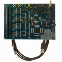
Manufacturer Part Number
CDB5376
Description
EVALUATION BOARD FOR CS5376
Manufacturer
Cirrus Logic Inc
Datasheets
1.CS5371A-ISZR.pdf
(32 pages)
2.CS4373A-ISZ.pdf
(34 pages)
3.CS5376A-IQZR.pdf
(106 pages)
4.CDB5378.pdf
(16 pages)
5.CDB5376.pdf
(80 pages)
6.CDB5376.pdf
(16 pages)
Specifications of CDB5376
Main Purpose
Seismic Evaluation System
Embedded
Yes, MCU, 8-Bit
Utilized Ic / Part
CS3301A, CS3302A, CS4373A, CS5372A, CS5376A
Primary Attributes
Quad Digital Filter
Secondary Attributes
Graphical User Interface, SPI™ & USB Interfaces
Processor To Be Evaluated
CS330x, CS4373A, CS537x
Interface Type
USB
Lead Free Status / RoHS Status
Contains lead / RoHS non-compliant
Lead Free Status / RoHS Status
Lead free / RoHS Compliant, Contains lead / RoHS non-compliant
Other names
598-1778


10. PIN DESCRIPTION - CS5372A
Power Supplies
VA+
VA-
VD
GND
Analog Inputs
INR1+, INR2+
INF1+, INF2+
INF1-, INF2-
INR1-, INR2-
DS748F3
Negative Voltage Reference Input
Positive Voltage Reference Input
Ch. 1 Rough Non-Inverting Input
Ch. 2 Rough Non-Inverting Input
_
_
Negative Analog Power Supply
_
Ch. 1 Fine Non-Inverting Input
Ch. 2 Fine Non-Inverting Input
Positive Analog Power Supply
Positive Digital Power Supply, pin 18
_
Negative Analog Power Supply, pin 7
Rough non-inverting analog inputs. The rough inputs settle non-linear currents to improve
linearity on the fine inputs and reduce harmonic distortion.
Fine non-inverting analog inputs.
Fine inverting analog inputs.
Rough inverting analog inputs. The rough inputs settle non-linear currents to improve linearity
on the fine inputs and reduce harmonic distortion.
Positive Analog Power Supply, pin 8
Ch. 1 Rough Inverting Input
Ch. 2 Rough Inverting Input
Ground, pin 17, 23
Ch. 1 Fine Inverting Input
Ch. 2 Fine Inverting Input
_
_
_
_
Channel 1 & 2 Fine Inverting Input, pin 3, 10
Channel 1 & 2 Rough Inverting Inputs, pin 4, 9
Channel 1 & 2 Fine Non-Inverting Input, pin 2, 11
Channel 1 & 2 Rough Non-Inverting Inputs, pin 1, 12
VREF+
VREF-
INR1+
INR2+
INF1+
INF2+
INR1-
INR2-
INF1-
INF2-
VA+
VA-
1
2
3
4
5
6
7
8
9
10
11
12
24
23
22
21
20
19
18
17
16
15
14
13
PWDN1
GND
MFLAG1
MDATA1
MSYNC
MCLK
VD
GND
MDATA2
MFLAG2
OFST
PWDN2
CS5371A CS5372A
Ch. 1 Power-down Enable
Digital Ground
Ch. 1 Modulator Flag Output
Ch. 1 Modulator Data Output
Modulator Sync Input
Modulator Clock Input
Positive Digital Power Supply
Digital Ground
Ch. 2 Modulator Data Output
Ch. 2 Modulator Flag Output
Offset Mode Select
Ch. 2 Power-down Enable
27
Related parts for CDB5376
Image
Part Number
Description
Manufacturer
Datasheet
Request
R

Part Number:
Description:
Development Kit
Manufacturer:
Cirrus Logic Inc
Datasheet:
Part Number:
Description:
Development Kit
Manufacturer:
Cirrus Logic Inc
Datasheet:


Part Number:
Description:
High-efficiency PFC + Fluorescent Lamp Driver Reference Design
Manufacturer:
Cirrus Logic Inc
Datasheet:
Part Number:
Description:
Development Kit
Manufacturer:
Cirrus Logic Inc
Datasheet:
Part Number:
Description:
Development Kit
Manufacturer:
Cirrus Logic Inc
Datasheet:

Part Number:
Description:
Development Kit
Manufacturer:
Cirrus Logic Inc
Datasheet:
Part Number:
Description:
Development Kit
Manufacturer:
Cirrus Logic Inc
Datasheet:
Part Number:
Description:
Development Kit
Manufacturer:
Cirrus Logic Inc
Datasheet:
Part Number:
Description:
Development Kit
Manufacturer:
Cirrus Logic Inc
Datasheet:

Part Number:
Description:
EVALUATION BOARD FOR CS8427
Manufacturer:
Cirrus Logic Inc
Datasheet:

Part Number:
Description:
BOARD EVAL FOR CS8416 RCVR
Manufacturer:
Cirrus Logic Inc
Datasheet:

Part Number:
Description:
EVALUATION BOARD FOR CS8420
Manufacturer:
Cirrus Logic Inc
Datasheet:

Part Number:
Description:
KIT DEVELOPMENT EP9315 ARM9
Manufacturer:
Cirrus Logic Inc
Datasheet:

Part Number:
Description:
KIT DEVELOPMENT EP9302 ARM9
Manufacturer:
Cirrus Logic Inc
Datasheet: