EVAL-AD7734EBZ Analog Devices Inc, EVAL-AD7734EBZ Datasheet - Page 19
EVAL-AD7734EBZ
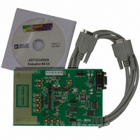
Manufacturer Part Number
EVAL-AD7734EBZ
Description
BOARD EVALUATION FOR AD7734
Manufacturer
Analog Devices Inc
Datasheet
1.AD7734BRUZ-REEL.pdf
(32 pages)
Specifications of EVAL-AD7734EBZ
Number Of Adc's
1
Number Of Bits
24
Sampling Rate (per Second)
15.4k
Data Interface
Serial
Inputs Per Adc
4 Single Ended
Input Range
±10 V
Power (typ) @ Conditions
85mW @ 5 V
Voltage Supply Source
Analog and Digital
Operating Temperature
-40°C ~ 105°C
Utilized Ic / Part
AD7734
Silicon Manufacturer
Analog Devices
Application Sub Type
ADC
Kit Application Type
Data Converter
Silicon Core Number
AD7734
Kit Contents
Board
Development Tool Type
Hardware - Eval/Demo Board
Rohs Compliant
Yes
Lead Free Status / RoHS Status
Lead free / RoHS Compliant


Channel Setup Registers
8 Bits, Read/Write Register, Address 28h–2Bh, Default Value 00h
These registers are used to configure the selected channel, to configure its input voltage range, and to set up the corresponding channel
status register.
Bit
Mnemonic
Default
Bit
7–5
4
3
2
1–0
Table 15.
RNG1
0
0
1
1
Channel Conversion Time Registers
8 Bits, Read/Write Register, Address 30h–33h, Default Value 91h
The conversion time registers enable or disable chopping and configure the digital filter for a particular channel. This register value affects
the conversion time, frequency response, and noise performance of the ADC.
Bit
Mnemonic
Default
Bit
7
6–0
Mnemonic
CHOP
FW
Mnemonic
0
Stat OPT
ENABLE
0
RNG1–RNG0
RNG0
0
1
0
1
±10 V
0 V to +10 V
±5 V
0 V to +5 V
Nominal Input Voltage Range
Bit 7
0
Description
These bits must be 0 for proper operation.
Status Option. When this bit is set to 1, the P0 and P1 bits in the channel status register will reflect the state of
the P0 and P1 pins. When this bit is reset to 0, the RDY bit in the channel status register will reflect the channel
corresponding to the RDY bit in the ADC status register.
Channel Enable. Set this bit to 1 to enable the channel in the continuous conversion mode. A single conversion
will take place regardless of this bit’s value.
This bit must be 0 for proper operation.
This is the channel input voltage range (see Table 15).
Bit 7
CHOP
1
Description
Chopping Enable Bit. Set to 1 to apply chopping mode for a particular channel.
CHOP = 1, single conversion or continuous conversion with one channel enabled.
Conversion Time (µs) = (FW × 128 + 248)/MCLK Frequency (MHz), the FW range is 2 to 127.
CHOP = 1, continuous conversion with two or more channels enabled.
Conversion Time (µs) = (FW × 128 + 249)/MCLK Frequency (MHz), the FW range is 2 to 127.
CHOP = 0, single conversion or continuous conversion with one channel enabled.
Conversion Time (µs) = (FW × 64 + 206)/MCLK Frequency (MHz), the FW range is 3 to 127.
CHOP = 0, continuous conversion with two or more channels enabled.
Conversion Time (µs) = (FW × 64 + 207)/MCLK Frequency (MHz), the FW range is 3 to 127.
0
Bit 6
0
0
Bit 6
Bit 5
0
0
Bit 5
Rev. 0 | Page 19 of 32
Stat OPT
Bit 4
0
Bit 4
FW (7-Bit Filter Word)
Bit 3
ENABLE
0
Bit 3
11h
Bit 2
0
0
Bit 2
Bit 1
RNG1
0
Bit 1
AD7734
Bit 0
RNG0
0
Bit 0
Related parts for EVAL-AD7734EBZ
Image
Part Number
Description
Manufacturer
Datasheet
Request
R


Part Number:
Description:
BOARD EVAL FOR SI270X-A
Manufacturer:
Silicon Laboratories Inc
Datasheet:

Part Number:
Description:
BUCK CONV REF DESIGN KIT IP1201
Manufacturer:
International Rectifier
Datasheet:
Part Number:
Description:
BOARD DEMO SYNC DUAL BUCK CNVTER
Manufacturer:
International Rectifier
Datasheet:
Part Number:
Description:
BOARD DEMO SYNC BUCK CONVETER
Manufacturer:
International Rectifier
Datasheet:

Part Number:
Description:
EVALBOARD/EB Omnidirectional microphone - Analog
Manufacturer:
Analog Devices
Datasheet:
Part Number:
Description:
EVALBOARD/EB Omnidirectional microphone - Analog
Manufacturer:
Analog Devices
Datasheet:


Part Number:
Description:
BOARD EVAL LED DRIVER LT3756
Manufacturer:
Linear Technology
Datasheet:

Part Number:
Description:
BOARD EVAL FOR AD7741/7742
Manufacturer:
Analog Devices Inc
Datasheet:

Part Number:
Description:
±1.7g Dual-Axis IMEMS Accelerometer Evaluation Board
Manufacturer:
Analog Devices Inc
Datasheet:

Part Number:
Description:
IC MULTIPLIER ANALOG 8-SOIC T/R
Manufacturer:
Analog Devices Inc
Datasheet:

Part Number:
Description:
IC ANALOG MULTIPLIER 8-DIP
Manufacturer:
Analog Devices Inc
Datasheet:
Part Number:
Description:
IC ANALOG MULTIPLIER 8-SOIC
Manufacturer:
Analog Devices Inc
Datasheet:
Part Number:
Description:
IC ANALOG MULTIPLIER 8-DIP
Manufacturer:
Analog Devices Inc
Datasheet: