ADC121C02XEB/NOPB National Semiconductor, ADC121C02XEB/NOPB Datasheet - Page 5
ADC121C02XEB/NOPB
Manufacturer Part Number
ADC121C02XEB/NOPB
Description
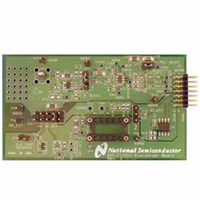
BOARD EVAL FOR ADC121C-21
Manufacturer
National Semiconductor
Series
PowerWise®r
Specifications of ADC121C02XEB/NOPB
Number Of Adc's
1
Number Of Bits
12
Sampling Rate (per Second)
188.9k
Data Interface
Serial
Inputs Per Adc
1 Single Ended
Input Range
0 ~ 5.5 V
Power (typ) @ Conditions
3.67mw @ 188.9kSPS
Voltage Supply Source
Single Supply
Operating Temperature
-40°C ~ 105°C
Utilized Ic / Part
ADC121C021,ADC121C027
Silicon Manufacturer
National
Silicon Core Number
ADC121C021, ADC121C027
Kit Application Type
Data Converter
Application Sub Type
ADC
Kit Contents
Board
Lead Free Status / RoHS Status
Lead free / RoHS Compliant
Other names
ADC121C02XEB


The LM4050-4.1 Precision, Micropower, Shunt
Voltage
ADC121C02XEB as a clean reference solution for
the ADC.
LM4050, simply short pins 1 & 2 of JP7, and move
the VA_SELECT jumper to pins 7 & 8 of JP5
(Figure 5).
3.0 Quick Start
The ADC121C02XEB evaluation board may be
used in the Stand Alone mode to capture data
with a logic analyzer or third party equipment, or it
may be used in the Computer Mode with a
WaveVision 4 Data Capture Board, referenced
throughout the remainder of this document as
WV4. In both cases, the data may be analyzed
with the WaveVision software.
3.1 Stand Alone Mode
Refer to Figure 1 for locations of test points and
major components.
1. The I
2. The board provides the option of adding 2kΩ
3. Connect a clean analog (not switching) +5.0V
5
be driven directly at J1 or with wires soldered
to VIA1 and VIA2 (step 7). A fully-compliant
I
SCL and SDA while monitoring the data
output (SDA).
pull-up resistors to the I
To enable the pull-up resistors, short pins 1 &
2 of JP2.
built-in pull-up resistors, the jumper at JP2
must be removed to disable the on-board pull-
up resistors. If the I
built-in pull-up capability, leave JP2 shorted.
power source with a 300mA current limit to
power connector TP7. Ground TP6.
2
C interface analyzer should be used to drive
Figure 5: LM4050 Jumper Configuration
2
C interface signals (SCL and SDA) may
Reference
To evaluate the ADC using the
Assuming the I
is
2
C analyzer doesn’t have
2
C bus, SCL and SDA.
included
2
C analyzer has
on
the
4. Move the shorting jumper at JP5 to pins 9 &
5. Turn on the power supply.
6. Connect the input signal to the test-point at
7. If evaluating the ADC121C027, configure the
8. If evaluating the ADC121C021, the slave
9. If evaluating the ADC121C021, the ALERT
3.2 Computer Mode
Refer to Figure 1 for locations of test points and
major components. The board comes configured
for “plug-and-play” WaveVision evaluation.
1. Run the WaveVision 4 program, version 4.4 or
2. Connect a USB cable between the WV4
3. Make
10. NOTE: only two consecutive pins may be
shorted on JP5 at a time.
J2. The input signal return can be connected
to ground at TP3. Please note the evaluation
board is assembled for a DC-coupled input
source.
coupled input as well. Modifying the board for
an AC coupled input is described above in
Section 2.0. If the source has a 50 ohm output
impedance, install a 51 ohm resistor at R3.
To
performance of the ADC121C021, the source
must be better than 90dB THD.
I
by VIA5. With VIA5 left floating, the slave
address of the ADC121C027 will be set to
50hex. Grounding VIA5 sets the address to
51hex. Connecting VIA5 to V
address to 52hex.
address is permanently set to 54hex.
pin can be monitored at VIA5.
higher is required to interface to the WV4
board. While the program is loading, continue
below.
board and the PC running the WaveVision 4
software.
connections, see table 1 for more details:
2
C slave address. The address is controlled
JP1 - pins 1 & 2
JP2 - pins 1 & 2
JP5 - pins 3 & 4 (All other pins of JP5
must be left open)
accurately
the
The board is designed for an AC
following
evaluate
http://www.national.com
required
the
A
sets the
dynamic
jumper
Related parts for ADC121C02XEB/NOPB
Image
Part Number
Description
Manufacturer
Datasheet
Request
R

Part Number:
Description:
National Semiconductor [8-Bit D/A Converter]
Manufacturer:
National Semiconductor
Datasheet:
Part Number:
Description:
National Semiconductor [Media Coprocessor]
Manufacturer:
National Semiconductor
Datasheet:
Part Number:
Description:
Digitally Controlled Tone and Volume Circuit with Stereo Audio Power Amplifier, Microphone Preamp Stage and National 3D Sound
Manufacturer:
National Semiconductor
Datasheet:
Part Number:
Description:
Digitally Controlled Tone and Volume Circuit with Stereo Audio Power Amplifier, Microphone Preamp Stage and National 3D Sound
Manufacturer:
National Semiconductor
Datasheet:
Part Number:
Description:
AC97 Rev 2 Codec with Sample Rate Conversion and National 3D Sound
Manufacturer:
National Semiconductor
Part Number:
Description:
Manufacturer:
National Semiconductor
Datasheet:
Part Number:
Description:
Manufacturer:
National Semiconductor
Datasheet:
Part Number:
Description:
General Purpose, Low Voltage, Low Power, Rail-to-Rail Output Operational Amplifiers
Manufacturer:
National Semiconductor
Datasheet:
Part Number:
Description:
8-bit 20 MSPS flash A/D converter.
Manufacturer:
National Semiconductor
Datasheet:
Part Number:
Description:
Low Noise Quad Operational Amplifier
Manufacturer:
National Semiconductor
Datasheet:
Part Number:
Description:
Quad Differential Line Receivers
Manufacturer:
National Semiconductor
Datasheet:
Part Number:
Description:
Quad High Speed Trapezoidal? Bus Transceiver
Manufacturer:
National Semiconductor
Datasheet:
Part Number:
Description:
Dual Line Receiver
Manufacturer:
National Semiconductor
Datasheet:
Part Number:
Description:
TTL to 10k ECL Level Translator with Latch
Manufacturer:
National Semiconductor
Datasheet: