ADC121C02XEB/NOPB National Semiconductor, ADC121C02XEB/NOPB Datasheet - Page 7
ADC121C02XEB/NOPB
Manufacturer Part Number
ADC121C02XEB/NOPB
Description
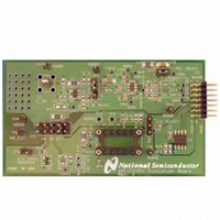
BOARD EVAL FOR ADC121C-21
Manufacturer
National Semiconductor
Series
PowerWise®r
Specifications of ADC121C02XEB/NOPB
Number Of Adc's
1
Number Of Bits
12
Sampling Rate (per Second)
188.9k
Data Interface
Serial
Inputs Per Adc
1 Single Ended
Input Range
0 ~ 5.5 V
Power (typ) @ Conditions
3.67mw @ 188.9kSPS
Voltage Supply Source
Single Supply
Operating Temperature
-40°C ~ 105°C
Utilized Ic / Part
ADC121C021,ADC121C027
Silicon Manufacturer
National
Silicon Core Number
ADC121C021, ADC121C027
Kit Application Type
Data Converter
Application Sub Type
ADC
Kit Contents
Board
Lead Free Status / RoHS Status
Lead free / RoHS Compliant
Other names
ADC121C02XEB


4.2 Analog Input Signal
There are three basic options for connecting an
input signal to the ADC.
facilitate
signals.
The first way to apply an input signal to the ADC
is to connect it to pin 2 of JP1. The signal’s return
(GND) should be connected to TP5.
configuration provides the input circuit seen in
Figure 8.
The second way is to configure the board for an
AC coupled input.
inputs applied to J2 but is currently not populated
on the board. By adding DC bias resistors R1 and
R4 (value 4.99kΩ), and changing C1 to a 1.0uF
capacitor, the board can be used with an AC
coupled input signal (Figure 3). To improve the
signal integrity of the connection to the board, an
SMA connector should be stuffed at J2 (V_IN). If
the input source has a 50Ω output impedance, a
51Ω resistor can be installed at R3.
The third way to configure the input is by
incorporating the Amplifier into the signal path.
The LMP7731 Low-noise, Precision Operational
Amplifier is included on the board for convenient
buffering of the analog input.
configured as a simple voltage follower (Figure 4).
Resistors R10 and R11 can be modified to add
non-inverting
capacitance at C6 configures the amplifier as a
low-pass filter.
move the JP1 jumper to pins 2 & 3.
In any case, it is important that the signal stays
within the allowable input range of the ADC (0V to
V
through a bandpass filter to eliminate the noise
and harmonics commonly associated with signal
sources. To accurately evaluate the performance
of the ADC121C021, the source must be better
than -90dBc THD.
7
A
). Dynamic input signals should be applied
AC-coupled
Figure 8: Unbiased input circuit.
gain
To use the input buffer, simply
DC biasing is available for
to
and
the
The three options
DC-coupled
circuit.
By default, it is
Adding
input
This
4.3 ADC Reference Circuitry
The ADC121C021 family is internally referenced.
Therefore, the Analog-to-Digital converter gets its
reference from the analog supply (V
clean analog supply must be used to guarantee
the performance of the ADC.
4.4 I
Please refer to section 1.7 of the ADC121C021
datasheet for a detailed description of the I
interface.
The board is designed with I
both the SDA and SCL lines (R8 & R9). These
resistors are enabled by a single jumper (JP2)
and can easily be added or removed from the I
bus.
designed into the board (R2 & R5). The board is
shipped with 0Ω resistors which can be modified
to provide series resistance if interfacing to a
noisy I
The SDA signal is accessible by soldering to VIA1
or connecting to pin 1 of the WV4S connector
(J1). The SCL signal is accessible by soldering to
VIA2 or connecting to pin 5 of J1.
The on-board pull-up resistors can be powered
with an external supply by removing the jumper at
JP2 and connecting the supply to pin 2 of JP2 or
VIA6.
4.5 Alert Function
The ADC121C021 provides a programmable “out-
of-range” Alert function.
conversion, the measured voltage is compared to
the values in the V
measured voltage violates either of these values,
an alert condition occurs. The Over Range Alert
flag in the Alert Status Register indicates the V
limit has been violated. The Under Range Alert
flag indicated the V
enabled, the alert condition is also propagated to
bit15 of the Conversion Result Register and the
ALERT output pin.
The Alert function is configured by writing to the
ADC’s internal registers. Refer to Section 1.6 of
the Datasheet for a detailed description of the
ADC’s internal Registers.
Refer to Section 1.8 of the Datasheet for a
detailed description of the Alert function.
2
C Interface
2
C bus.
Also, footprints for series resistors are
HIGH
LOW
and V
limit has been violated. If
At the end of every
2
C pull-up resistors on
LOW
http://www.national.com
registers. If the
A
). Hence, a
HIGH
2
2
C
C
Related parts for ADC121C02XEB/NOPB
Image
Part Number
Description
Manufacturer
Datasheet
Request
R

Part Number:
Description:
National Semiconductor [8-Bit D/A Converter]
Manufacturer:
National Semiconductor
Datasheet:
Part Number:
Description:
National Semiconductor [Media Coprocessor]
Manufacturer:
National Semiconductor
Datasheet:
Part Number:
Description:
Digitally Controlled Tone and Volume Circuit with Stereo Audio Power Amplifier, Microphone Preamp Stage and National 3D Sound
Manufacturer:
National Semiconductor
Datasheet:
Part Number:
Description:
Digitally Controlled Tone and Volume Circuit with Stereo Audio Power Amplifier, Microphone Preamp Stage and National 3D Sound
Manufacturer:
National Semiconductor
Datasheet:
Part Number:
Description:
AC97 Rev 2 Codec with Sample Rate Conversion and National 3D Sound
Manufacturer:
National Semiconductor
Part Number:
Description:
Manufacturer:
National Semiconductor
Datasheet:
Part Number:
Description:
Manufacturer:
National Semiconductor
Datasheet:
Part Number:
Description:
General Purpose, Low Voltage, Low Power, Rail-to-Rail Output Operational Amplifiers
Manufacturer:
National Semiconductor
Datasheet:
Part Number:
Description:
8-bit 20 MSPS flash A/D converter.
Manufacturer:
National Semiconductor
Datasheet:
Part Number:
Description:
Low Noise Quad Operational Amplifier
Manufacturer:
National Semiconductor
Datasheet:
Part Number:
Description:
Quad Differential Line Receivers
Manufacturer:
National Semiconductor
Datasheet:
Part Number:
Description:
Quad High Speed Trapezoidal? Bus Transceiver
Manufacturer:
National Semiconductor
Datasheet:
Part Number:
Description:
Dual Line Receiver
Manufacturer:
National Semiconductor
Datasheet:
Part Number:
Description:
TTL to 10k ECL Level Translator with Latch
Manufacturer:
National Semiconductor
Datasheet: