STEVAL-PSQ001V1 STMicroelectronics, STEVAL-PSQ001V1 Datasheet - Page 39
STEVAL-PSQ001V1
Manufacturer Part Number
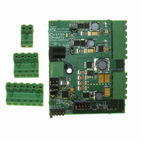
STEVAL-PSQ001V1
Description
BOARD EVAL BASED ON PM6680A
Manufacturer
STMicroelectronics
Type
Other Power Managementr
Specifications of STEVAL-PSQ001V1
Design Resources
STEVAL-PSQ001V1 Gerber Files STEVAL-PSQ001V1 Schematic STEVAL-PSQ001V1 Bill of Material
Main Purpose
DC/DC, Step Down with LDO
Outputs And Type
6, Non-Isolated
Voltage - Output
0.9 ~ 2.5 V, 1 ~ 3.3 V, 2x 3.3 V, 2.5 V, 5 V
Current - Output
4A, 2A, 800mA, 400mA, 400mA, 150mA
Voltage - Input
5 ~ 36V
Regulator Topology
Buck
Frequency - Switching
200kHz, 300kHz
Board Type
Fully Populated
Utilized Ic / Part
PM6680A
Input Voltage
5 V to 36 V
Output Voltage
1 V to 3.3 V
Product
Power Management Modules
Silicon Manufacturer
ST Micro
Silicon Core Number
PM6680A
Kit Application Type
Power Management
Application Sub Type
Power Supply
Kit Contents
Board
Rohs Compliant
Yes
Lead Free Status / RoHS Status
Lead free / RoHS Compliant
Power - Output
-
Lead Free Status / Rohs Status
Lead free / RoHS Compliant
For Use With/related Products
PM6680A
Other names
497-6425
STEVAL-PSQ001V1
STEVAL-PSQ001V1


PM6680A
9.7
Other parts design
●
Figure 38. VIN pin filter
Typical components values are: R = 3.9 Ω and C = 4.7 µF.
●
Figure 39. Inductor current waveforms
Typical components values are: R = 47 Ω and C = 1µF.
●
●
●
VIN filter
A VIN pin low pass filter is suggested to reduce switching noise. The low pass filter is
shown in the next figure:
VCC filter
A VCC low pass filter helps to reject switching commutations noise:
VREF capacitor
A 10nF to 100nF ceramic capacitor on VREF pin must be added to ensure noise
rejection.
LDO5 output capacitors
Bypass the output of each linear regulator with 1 µF ceramic capacitor closer to the
LDO pin and a 4.7µF tantalum capacitor (ESR = 2 Ω). In most applicative conditions a
4.7 µF ceramic output capacitor can be enough to ensure stability.
Bootstrap circuit
The external bootstrap circuit is represented in the next figure:
Input
voltage
R
R
C
C
R
R
C
C
1
1
0
0
0
0
p
p
F
F
L
V
L
V
V
V
D
D
C
C
I
I
N
N
O
O
C
C
5
5
Design guidelines
39/48
Related parts for STEVAL-PSQ001V1
Image
Part Number
Description
Manufacturer
Datasheet
Request
R

Part Number:
Description:
BOARD ELECT FISCAL CASH REGISTER
Manufacturer:
STMicroelectronics
Datasheet:

Part Number:
Description:
BOARD DEMO LNB PS LNBH23L QFN
Manufacturer:
STMicroelectronics
Datasheet:

Part Number:
Description:
BOARD DEMONSTRATION LNBH PS
Manufacturer:
STMicroelectronics
Datasheet:

Part Number:
Description:
BOARD EVAL FOR MEMS SENSORS
Manufacturer:
STMicroelectronics
Datasheet:
Part Number:
Description:
EVALBOARD/STEVAL-ISV014V1
Manufacturer:
STMicroelectronics
Part Number:
Description:
BOARD EVAL FOR ST802RT1
Manufacturer:
STMicroelectronics
Datasheet:

Part Number:
Description:
BOARD EVAL FOR VACUUM CLEANER
Manufacturer:
STMicroelectronics
Datasheet:

Part Number:
Description:
KIT DEV STARTER ST10F276Z5
Manufacturer:
STMicroelectronics
Datasheet:

Part Number:
Description:
BOARD LED CTLR/DVR STLED316S
Manufacturer:
STMicroelectronics
Datasheet:

Part Number:
Description:
BOARD EVAL BLDC SENSORLESS MOTOR
Manufacturer:
STMicroelectronics
Datasheet:
Part Number:
Description:
STMicroelectronics [RIPPLE-CARRY BINARY COUNTER/DIVIDERS]
Manufacturer:
STMicroelectronics
Datasheet:
Part Number:
Description:
STMicroelectronics [LIQUID-CRYSTAL DISPLAY DRIVERS]
Manufacturer:
STMicroelectronics
Datasheet:
Part Number:
Description:
BOARD EVAL FOR MEMS SENSORS
Manufacturer:
STMicroelectronics
Datasheet: