RDK-83 Power Integrations, RDK-83 Datasheet - Page 8
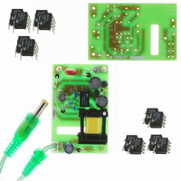
RDK-83
Manufacturer Part Number
RDK-83
Description
KIT DESIGN REF LINKSWITCH LP
Manufacturer
Power Integrations
Series
LinkSwitch®-LPr
Specifications of RDK-83
Main Purpose
AC/DC, Primary Side
Outputs And Type
1, Isolated
Power - Output
1.6W
Voltage - Output
7.7V
Current - Output
210mA
Voltage - Input
85 ~ 265VAC
Regulator Topology
Flyback
Frequency - Switching
66kHz
Board Type
Bare (Unpopulated) and Fully Populated
Utilized Ic / Part
LNK562, LNK563, LNK564
Lead Free Status / RoHS Status
Not applicable / Not applicable
Other names
596-1128


The LinkSwitch-LP family of ICs are self-biased, via a high-voltage current source that is
internally connected to the DRAIN pin of the package. A capacitor (C2) connected to the
BYPASS (BP) pin of the IC provides energy storage and local decoupling of the internal
chip power. To further reduce no-load power consumption, a resistor can be used to
provide operating current to the IC from the bias winding (once the power supply is
operating). In this design, the bias winding voltage is about 14 V and the BP pin voltage
is 5.8 V. Therefore, R6 (100 kΩ) provides about 80 µA of current to the BP pin. If the
value of R6 were reduced, it could provide the entire 220 µA of IC supply current, which
would further reduce the no-load power consumption of the supply.
The worst-case, no-load power consumption of this supply is approximately 200 mW at
an input voltage of 265 VAC, which is well below the maximum limit of most energy
efficiency standards. Heat generation is also kept to a minimum in this design, given the
high operating efficiency at all line and load conditions.
4.3 Feedback
The output voltage of the supply is regulated based on feedback from the primary-side
bias supply. The bias winding voltage is rectified and filtered by D3 and C3. The leakage
inductance between the output winding and the bias winding induces error in the bias
winding voltage. Using a standard rectifier diode for D3 makes the bias winding voltage
more accurately track the output voltage. Resistor R7 preloads (3 mA) the output of the
bias supply, which further reduces the error and also limits the no-load output voltage.
A resistor divider (R1 and R2) provides the feedback voltage to the FB pin of U1. The
values of R1 and R2 are selected so that when the output voltage is at the desired
nominal value, the voltage on the FB pin is 1.69 V, and about 70 µA flows into the FB pin.
The LinkSwitch-LP family of devices use ON/OFF control to regulate the output of the
supply. During constant voltage (CV) operation, switching cycles are skipped when the
current into the FB pin exceeds 70 µA. As the load on the output of the supply reduces,
more switching cycles are skipped. As the load increases, fewer cycles are skipped.
The result is that the average or effective switching frequency varies with the load. This
makes the efficiency fairly consistent over the entire load range, since the switching
losses scale with the load on the output of the supply.
When the load on the output of the supply reaches its maximum power capability, no
switching cycles are skipped. If the load is increased beyond that point, the output
voltage of the supply will start to drop. As the output voltage drops, the voltage on the FB
pin also drops, and the IC linearly reduces its switching frequency. This keeps the output
current from increasing significantly. Once the FB pin voltage falls below 0.8 V for more
than 100 ms, all LinkSwitch-LP devices enter an auto-restart mode. While in auto-restart,
the controller enables MOSFET switching for 100 ms. If the FB pin voltage does not
exceed 0.8 V during the 100 ms, the controller disables MOSFET switching. MOSFET
switching is alternately enabled and disables at a duty cycle of about 12% until the fault
condition clears. This protects both the supply and the load.
Power Integrations
Tel: +1 408 414 9200 Fax: +1 408 414 9201
www.powerint.com
Page 8 of 36
Related parts for RDK-83
Image
Part Number
Description
Manufacturer
Datasheet
Request
R

Part Number:
Description:
KIT REF DESIGN 36-72W MOTOR DRVR
Manufacturer:
Power Integrations
Datasheet:

Part Number:
Description:
KIT REF DESIGN FOR LNK457D
Manufacturer:
Power Integrations
Datasheet:

Part Number:
Description:
REFERENCE DESIGN LINKSWITCH-PH
Manufacturer:
Power Integrations
Datasheet:

Part Number:
Description:
Specifications: Manufacturer: Power Integrations ; Output Voltage: 380 VDC ; Input / Supply Voltage (Max): 264 VAC ; Input / Supply Voltage (Min): 90 VAC ; Mounting Style: Through Hole ; Output Current: 0.913 A ; Output Power: 347 W
Manufacturer:
Power Integrations, Inc.

Part Number:
Description:
KIT REF DESIGN TOP HX FOR TOP258
Manufacturer:
Power Integrations
Datasheet:

Part Number:
Description:
Power Management Modules & Development Tools TOPSwitch-JX REF. DESIGN KIT
Manufacturer:
Power Integrations
Datasheet:
Part Number:
Description:
Power Management IC Development Tools REF DESIGN RDR-292 PFF LED STREET LIGHT
Manufacturer:
Power Integrations

Part Number:
Description:
KIT REF DESIGN FOR LNK403EG
Manufacturer:
Power Integrations
Datasheet:

Part Number:
Description:
KIT REF DESIGN FOR LNK406EG
Manufacturer:
Power Integrations
Datasheet:

Part Number:
Description:
KIT REF DESIGN DG CAPZERO
Manufacturer:
Power Integrations
Datasheet:

Part Number:
Description:
KIT REF DESIGN LINKSWITCH-CV
Manufacturer:
Power Integrations
Datasheet:

Part Number:
Description:
KIT REF DESIGN LINKSWITCH 2
Manufacturer:
Power Integrations
Datasheet:

Part Number:
Description:
KIT REF DESIGN PFS762HG
Manufacturer:
Power Integrations
Datasheet:
Part Number:
Description:
Specifications: Family: Eval Boards - DC/DC & AC/DC (Off-Line) SMPS ; Series: HiperLCS™ ; Main Purpose: DC/DC, Step Down ; Outputs and Type: 1, Isolated ; Power - Output: 150W ; Voltage - Output: 24V ; Current - Output: 6.25A ; Voltage - Input:
Manufacturer:
Power Integrations, Inc.
Datasheet:

Part Number:
Description:
KIT REF DESIGN 1.2W PS TN FAMILY
Manufacturer:
Power Integrations
Datasheet: