MCP4728EV Microchip Technology, MCP4728EV Datasheet - Page 22
MCP4728EV
Manufacturer Part Number
MCP4728EV
Description
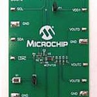
BOARD EVAL 12BIT 4CH DAC MCP4728
Manufacturer
Microchip Technology
Type
D/Ar
Specifications of MCP4728EV
Number Of Dac's
4
Number Of Bits
12
Outputs And Type
1, Single Ended
Data Interface
I²C
Settling Time
6µs
Dac Type
Voltage
Voltage Supply Source
Single
Operating Temperature
-40°C ~ 125°C
Utilized Ic / Part
MCP4728
Product
Data Conversion Development Tools
Resolution
12 bit
Interface Type
I2C
Supply Voltage (max)
5.5 V
Supply Voltage (min)
2.7 V
Silicon Manufacturer
Microchip
Silicon Core Number
MCP4728
Kit Application Type
Data Converter
Application Sub Type
DAC
Kit Contents
Board
For Use With/related Products
MCP4728
Lead Free Status / RoHS Status
Lead free / RoHS Compliant
Lead Free Status / RoHS Status
Lead free / RoHS Compliant, Lead free / RoHS Compliant
Available stocks
Company
Part Number
Manufacturer
Quantity
Price
Company:

Part Number:
MCP4728EV
Manufacturer:
Microchip Technology
Quantity:
135
Company:
Part Number:
MCP4728EV
Manufacturer:
MICROCHIP
Quantity:
12 000


MCP4728
3.3
SDA is the serial data pin of the I
pin is used to write or read the DAC register and
EEPROM data. Except for Start and Stop conditions,
the data on the SDA pin must be stable during the high
duration of the clock pulse. The High or Low state of the
SDA pin can only change when the clock signal on the
SCL pin is Low.
The SDA pin is an open-drain N-channel driver.
Therefore, it needs a pull-up resistor from the V
to the SDA pin.
Refer
Communications”
Interface communication.
3.4
This pin can be driven by an external control device
such as an MCU I/O pin. This pin is used to:
a)
b)
For more details on reading and writing the I
bits, see
Bits”
Address bits (C2=0, C1=1,
When the logic status of the LDAC pin changes from
“High” to “Low”, the contents of all input registers
(Channels A – D) are transferred to their corresponding
output registers, and all analog voltage outputs are
updated simultaneously.
If this pin is permanently tied to “Low”, the content of
the input register is transferred to its output register
(V
acknowledge pulse.
The user can also use the UDAC bit instead. However,
the UDAC bit updates a selected channel only. See
Section 4.8 “Output Voltage Update”
information on the LDAC pin and UDAC bit functions.
DS22187E-page 22
OUT
transfer the contents of the input registers to
their corresponding DAC output registers and
select a device of interest when reading or writ-
ing I
and
) immediately at the last input data byte’s
to
2
Serial Data Pin (SDA)
Section 5.4.4 “General Call Read Address
LDAC Pin
C address bits.
Section 5.6.8 “Write Command: Write I2C
Section 5.0
for more details on the I
“I
C0=1)”.
2
C
2
C interface. The SDA
Serial
2
C address
for more
Interface
2
C Serial
DD
line
3.5
This pin is a status indicator of EEPROM programming
activity. This pin is “High” when the EEPROM has no
programming activity, and “Low” when the EEPROM is
in programming mode. It goes “High” when the
EEPROM program is completed.
The RDY/BSY pin is an open-drain N-channel driver.
Therefore, it needs a pull-up resistor (about 100 kΩ)
from the V
if it is not used.
3.6
The device has four analog voltage output (V
Each output is driven by its own output buffer with a
gain of 1 or 2, depending on the gain and V
selection bit settings. In Normal mode, the DC
impedance of the output pin is about 1Ω. In
Power-Down mode, the output pin is internally
connected to 1 kΩ, 100 kΩ, or 500 kΩ, depending on
the Power-Down selection bit settings.
The V
load. It is recommended to use a load with R
than 5 kΩ.
OUT
RDY/BSY Status Indicator Pin
Analog Output Voltage Pins
(V
DD
pin can drive up to 1000 pF of capacitive
OUT
line to the RDY/BSY pin. Let this pin float
A
,
V
OUT
© 2010 Microchip Technology Inc.
B
,
V
OUT
C
,
V
OUT
OUT
L
greater
D)
) pins.
REF
Related parts for MCP4728EV
Image
Part Number
Description
Manufacturer
Datasheet
Request
R

Part Number:
Description:
Manufacturer:
Microchip Technology Inc.
Datasheet:
Part Number:
Description:
Manufacturer:
Microchip Technology Inc.
Datasheet:
Part Number:
Description:
Manufacturer:
Microchip Technology Inc.
Datasheet:
Part Number:
Description:
Manufacturer:
Microchip Technology Inc.
Datasheet:
Part Number:
Description:
Manufacturer:
Microchip Technology Inc.
Datasheet:
Part Number:
Description:
Manufacturer:
Microchip Technology Inc.
Datasheet:
Part Number:
Description:
Manufacturer:
Microchip Technology Inc.
Datasheet:
Part Number:
Description:
Manufacturer:
Microchip Technology Inc.
Datasheet: