DK86060-3 Fujitsu Semiconductor America Inc, DK86060-3 Datasheet - Page 27
DK86060-3
Manufacturer Part Number
DK86060-3
Description
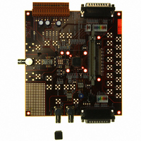
KIT DEV 16BIT DAC FOR MB86060
Manufacturer
Fujitsu Semiconductor America Inc
Specifications of DK86060-3
Number Of Dac's
1
Number Of Bits
16
Outputs And Type
1, Differential
Sampling Rate (per Second)
400M
Data Interface
Parallel
Dac Type
Current
Voltage Supply Source
Single
Operating Temperature
-40°C ~ 85°C
Utilized Ic / Part
MB86060
Lead Free Status / RoHS Status
Lead free / RoHS Compliant
Other names
865-1009


February 2009 Version 2.0
FME/MS/SFDAC1/DS/4250
MB86060 16-bit Interpolating Digital to Analog Converter
If a common, system wide logic level clock source is to be used, this should be transformer coupled
to remove common mode noise and isolate the clock ground region. The recommended 1:1
impedance transformer is a Mini-Circuits, ADT1-1. The secondary will be connected to the differential
clock inputs CLK and CLKB, and terminated with a 100
should be 50
source and the digital clock source ground. A 100 source resistor is used, and the PCB tracks to
the clock source should be 100 . See figure 16c.
For connection to a low noise RF source, a Balun transformer should be used. The recommended
transformer is a Mini-Circuits ADTL1-4-75. The secondary terminals should be connected through a
100nF capacitor to the differential clock inputs CLK and CLKB. The clock inputs should be terminated
with a 50 resistor. The primary dot should be connected to the RF signal with a 50 PCB track, and
the other primary connection should be connected to RF ground. The primary ground may be
connected to clock ground if necessary. See figure 16d. This configuration would allow for a RF
signal level of between -6dBm and +24dBm, giving a differential signal level of up to 5V pk-pk at CLK
and CLKB.
Copyright © 2003-2009 Fujitsu Microelectronics Europe GmbH
Disclaimer: The contents of this document are subject to change without notice. Customers are advised to consult with FUJITSU sales representatives before
System Ground
System clock
C: Using a common system clock source
CGND
A: Using the internal crystal oscillator
ordering.The information and circuit diagrams in this document are presented “as is”, no license is granted by implication or otherwise.
22pF
22pF
100
tracks. The primary of the transformer will be connected between the digital clock
1M
ADT1-1
XTAL
100
XIN
XOUT
Figure 16 Clock Input Configurations
MB86060
CLK
CLKB
MB86060
RF Source
RF Ground
B: Using a dedicated CMOS oscillator
resistor. The PCB tracks to the device
ADTL1-4-75
Production
OSC
CLKOUT
GND
D: Using an RF source
CGND
100nF
100nF
50
XIN
CVSS
MB86060
CLKB
CLK
Page 27 of 44
MB86060
Related parts for DK86060-3
Image
Part Number
Description
Manufacturer
Datasheet
Request
R

Part Number:
Description:
IC POWER SUPPLY MONITOR 8SOP
Manufacturer:
Fujitsu Semiconductor America Inc
Datasheet:
Part Number:
Description:
IC POWER SUPPLY MONITOR 8SOP
Manufacturer:
Fujitsu Semiconductor America Inc
Datasheet:

Part Number:
Description:
IC MCU 60K FLASH 2KB RAM 52LQFP
Manufacturer:
Fujitsu Semiconductor America Inc
Datasheet:

Part Number:
Description:
IC MCU 32BIT 256KB FLASH 120LQFP
Manufacturer:
Fujitsu Semiconductor America Inc
Datasheet:
Part Number:
Description:
IC CTLR TOUCH SENSOR 12CH 30SSOP
Manufacturer:
Fujitsu Semiconductor America Inc
Datasheet:

Part Number:
Description:
IC CTLR TOUCH SENSOR 12CH 40QFN
Manufacturer:
Fujitsu Semiconductor America Inc
Datasheet:
Part Number:
Description:
SYNTHESIZER PLL DUAL INP 20SSOP
Manufacturer:
Fujitsu Semiconductor America Inc
Datasheet:

Part Number:
Description:
SYNTHESZR PLL 1.1GHZ DUAL 16SSOP
Manufacturer:
Fujitsu Semiconductor America Inc
Datasheet:

Part Number:
Description:
IC SSCG EMI RED 8-SOIC
Manufacturer:
Fujitsu Semiconductor America Inc
Datasheet:

Part Number:
Description:
IC SSCG EMI RED 8-TSSOP
Manufacturer:
Fujitsu Semiconductor America Inc
Datasheet:

Part Number:
Description:
IC SSCG EMI RED 8-SOP
Manufacturer:
Fujitsu Semiconductor America Inc
Datasheet:

Part Number:
Description:
SYNTHESIZER PLL 2.5GHZ 16SSOP
Manufacturer:
Fujitsu Semiconductor America Inc
Datasheet:
Part Number:
Description:
SYNTHESIZER PLL 1.2GHZ 16SSOP
Manufacturer:
Fujitsu Semiconductor America Inc
Datasheet:

Part Number:
Description:
SYNTHESIZER PLL 2.5GHZ 16BCC
Manufacturer:
Fujitsu Semiconductor America Inc
Datasheet:

Part Number:
Description:
IC SSCG EMI RED 8-SOP
Manufacturer:
Fujitsu Semiconductor America Inc
Datasheet: