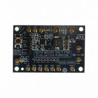
STEVAL-ISA056V1 STMicroelectronics, STEVAL-ISA056V1 Datasheet - Page 26
STEVAL-ISA056V1
Manufacturer Part Number
STEVAL-ISA056V1
Description
BOARD EVAL BASED ON PM6600
Manufacturer
STMicroelectronics
Type
PWM Controllersr
Specifications of STEVAL-ISA056V1
Design Resources
STEVAL-ISA056V1 Gerber Files STEVAL-ISA056V1 Schematic STEVAL-ISA056V1 Bill of Material
Current - Output / Channel
30mA
Outputs And Type
6, Non-Isolated
Voltage - Output
36 V
Features
Dimmable
Voltage - Input
4.5 ~ 28V
Utilized Ic / Part
PM6600
Input Voltage
4.5 V to 28 V
Output Voltage
36 V
Product
Power Management Modules
Core Chip
PM6600
Topology
Boost
No. Of Outputs
1
Dimming Control Type
PWM
Mcu Supported Families
PM6600
Lead Free Status / RoHS Status
Lead free / RoHS Compliant
For Use With/related Products
PM6600
Other names
497-8414
Available stocks
Company
Part Number
Manufacturer
Quantity
Price
Company:

Part Number:
STEVAL-ISA056V1
Manufacturer:
STMicroelectronics
Quantity:
1


Operation description
7
7.1
7.1.1
26/60
Operation description
Boost section
Functional description
The PM6600 is a monolithic LEDs driver for the backlight of LCD panels and it consists of a
boost converter and six PWM-dimmable current generators.
The input voltage range is from 4.7 V up to 28 V.
The boost section is based on a constant switching frequency, Peak Current-Mode
architecture. The boost output voltage is controlled such that the lowest ROWs' voltage,
referred to SGND, is equal to an internal reference voltage (400 mV typ.).
In addition, the PM6600 has an internal LDO that supplies the internal circuitry of the device
and is capable to deliver up to 40 mA. The input of the LDO is the VIN pin. The LDO5 pin is
the LDO output and the supply for the power-MOSFET driver at the same time. The AVCC
pin is the supply for the analog circuitry and should be connected to the LDO output through
a simple RC filter, in order to improve the noise rejection.
Figure 43. AVCC filtering
Two loops are involved in regulating the current sunk by the generators.
The main loop is related to the boost regulator and uses a constant frequency peak current-
mode architecture (see
at each ROW according to the set value (RILIM pin).
A dedicated circuit automatically selects the lowest voltage drop among all the ROWs and
provides this voltage the main loop that, in turn, regulates the output voltage. In fact, once
the reference generator has been detected, the error amplifier compares its voltage drop to
the internal reference voltage and varies the COMP output. The voltage at the COMP pin
determines the inductor peak current at each switching cycle. The output voltage of the
boost regulator is thus determined by the total forward voltage of the LEDs strings:
Equation 1
Figure
V
Doc ID 14248 Rev 7
49), while an internal current loop regulates the same current
Cavcc
100n
4R7
Rfilt
OUT
LDO5
AVCC
=
N
max
ROWS
i
=
1
(
m
Σ
LEDS
j
=
1
V
F
LDO
j ,
)
SGND
VIN
+
400
PM6600
mV
PM6600
Related parts for STEVAL-ISA056V1
Image
Part Number
Description
Manufacturer
Datasheet
Request
R

Part Number:
Description:
BOARD RGB CTR ST7,STP08C596MTR
Manufacturer:
STMicroelectronics
Datasheet:

Part Number:
Description:
Power Management IC Development Tools Full Speed USB to RS232 Bridge Demo
Manufacturer:
STMicroelectronics
Datasheet:
Part Number:
Description:
Power Management IC Development Tools 2.5W solar eval BRD USB SPV1040 LD39050
Manufacturer:
STMicroelectronics
Datasheet:

Part Number:
Description:
BOARD EVAL FOR MEMS SENSORS
Manufacturer:
STMicroelectronics
Datasheet:

Part Number:
Description:
KIT DEV STARTER ST10F276Z5
Manufacturer:
STMicroelectronics
Datasheet:

Part Number:
Description:
BOARD EVAL HDMI $ VIDEO SWITCH
Manufacturer:
STMicroelectronics
Datasheet:

Part Number:
Description:
BOARD DEMO ACCELEROMETER DIL24
Manufacturer:
STMicroelectronics
Datasheet:

Part Number:
Description:
BOARD STLM75/STDS75/ST72F651
Manufacturer:
STMicroelectronics
Datasheet:

Part Number:
Description:
EVAL BOARD 3AXIS MEMS ACCELLRMTR
Manufacturer:
STMicroelectronics
Datasheet:

Part Number:
Description:
BOARD EVAL 8BIT MICRO + TDE1708
Manufacturer:
STMicroelectronics
Datasheet:
Part Number:
Description:
STMicroelectronics [RIPPLE-CARRY BINARY COUNTER/DIVIDERS]
Manufacturer:
STMicroelectronics
Datasheet:
Part Number:
Description:
STMicroelectronics [LIQUID-CRYSTAL DISPLAY DRIVERS]
Manufacturer:
STMicroelectronics
Datasheet:
Part Number:
Description:
BOARD EVAL FOR MEMS SENSORS
Manufacturer:
STMicroelectronics
Datasheet: