TC1016/17EV Microchip Technology, TC1016/17EV Datasheet - Page 11
TC1016/17EV
Manufacturer Part Number
TC1016/17EV
Description
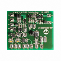
BOARD DEMO FOR TC1016/TC1017
Manufacturer
Microchip Technology
Specifications of TC1016/17EV
Design Resources
TC1016/17EV Gerber Files
Channels Per Ic
1 - Single
Voltage - Output
1.8V, 3V
Current - Output
150mA, 150mA
Voltage - Input
2.7 ~ 6V
Regulator Type
Positive Fixed
Operating Temperature
-40°C ~ 125°C
Board Type
Fully Populated
Utilized Ic / Part
TC1016, TC1017
Processor To Be Evaluated
TC1016 and TC1017
Lead Free Status / RoHS Status
Contains lead / RoHS non-compliant
Lead Free Status / RoHS Status
Lead free / RoHS Compliant, Contains lead / RoHS non-compliant


4.1
Low input source impedance is necessary for the LDO
to operate properly. When operating from batteries, or
in applications with long lead length (> 10") between
the input source and the LDO, some input capacitance
is required. A minimum of 0.1 µF is recommended for
most applications and the capacitor should be placed
as close to the input of the LDO as is practical. Larger
input capacitors will help reduce the input impedance
and further reduce any high-frequency noise on the
input and output of the LDO.
4.2
A minimum output capacitance of 1 µF for the TC1017
is required for stability. The Equivalent Series Resis-
tance (ESR) requirements on the output capacitor are
between 0 and 2 ohms. The output capacitor should be
located as close to the LDO output as is practical.
Ceramic materials X7R and X5R have low temperature
coefficients and are well within the acceptable ESR
range required. A typical 1 µF X5R 0805 capacitor has
an ESR of 50 milli-ohms. Larger output capacitors can
be used with the TC1017 to improve dynamic behavior
and input ripple-rejection performance.
Ceramic, aluminum electrolytic or tantalum capacitor
types can be used. Since many aluminum electrolytic
capacitors freeze at approximately –30 C, ceramic or
solid tantalums are recommended for applications
operating below –25 C. When operating from sources
other than batteries, supply-noise rejection and
transient response can be improved by increasing the
value of the input and output capacitors and employing
passive filtering techniques.
FIGURE 4-3:
© 2005 Microchip Technology Inc.
Input Capacitor
Output Capacitor
SHDN
V
OUT
Wake-Up Time from Shutdown.
V
IL
4.3
The turn-on response is defined as two separate
response categories, wake-up time (t
time (t
The TC1017 has a fast wake-up time (10 µsec, typical)
when released from shutdown. See Figure 4-3 for the
wake-up time designated as t
defined as the time it takes for the output to rise to 2%
of the V
The total turn-on response is defined as the settling
time (t
t
within 98% of its fully-enabled value (32 µsec, typical)
when released from shutdown. The settling time of the
output voltage is dependent on load conditions and
output capacitance on V
The table below demonstrates the typical turn-on
response timing for different input voltage power-up
frequencies: V
and C
WK
Frequency
) is defined as the condition when the output is
1000 Hz
500 Hz
100 Hz
OUT
50 Hz
10 Hz
S
S
) (see Figure 4-3). Settling time (inclusive with
).
OUT
Turn-On Response
= 1 µF.
2%
value after being released from shutdown.
OUT
t
WK
V
98%
IH
= 2.85V, V
Typical (t
14.5 µsec
17.2 µsec
5.3 µsec
5.9 µsec
9.8 µsec
OUT
t
S
(RC response).
WK
IN
WK
. The wake-up time is
= 5.0V, I
)
TC1017
DS21813D-page 11
WK
Typical (t
) and settling
OUT
14 µsec
16 µsec
32 µsec
52 µsec
77 µsec
= 60 mA
S
)
Related parts for TC1016/17EV
Image
Part Number
Description
Manufacturer
Datasheet
Request
R


Part Number:
Description:
IC REG LDO 3.0V 80MA SD SC-70-5
Manufacturer:
Microchip Technology
Datasheet:
Part Number:
Description:
IC REG LDO 3.3V 80MA SD SC70-5
Manufacturer:
Microchip Technology
Datasheet:

Part Number:
Description:
IC REG LDO 2.7V SOT-23-5
Manufacturer:
Microchip Technology
Datasheet:
Part Number:
Description:
IC REG LDO 1.8V 80MA SD SC-70-5
Manufacturer:
Microchip Technology
Datasheet:
Part Number:
Description:
IC REG LDO 1.85V SOT-23-5
Manufacturer:
Microchip Technology
Datasheet:
Part Number:
Description:
IC REG LDO 2.8V SOT-23-5
Manufacturer:
Microchip Technology
Datasheet:
Part Number:
Description:
IC REG LDO 4.0V SOT-23-5
Manufacturer:
Microchip Technology
Datasheet:
Part Number:
Description:
IC REG LDO 4.0V SC70-5
Manufacturer:
Microchip Technology
Datasheet:
Part Number:
Description:
IC CMOS LDO 80MA 3.3V SOT23-5
Manufacturer:
Microchip Technology
Datasheet:
Part Number:
Description:
IC CMOS LDO 80MA 1.8V SOT23-5
Manufacturer:
Microchip Technology
Datasheet:
Part Number:
Description:
IC REG LDO 2.8V 80MA SD SC-70-5
Manufacturer:
Microchip Technology
Datasheet:
Part Number:
Description:
IC REG LDO 2.7V 80MA SD SC-70-5
Manufacturer:
Microchip Technology
Datasheet:

Part Number:
Description:
80mA Tiny CMOS LDO With Shutdown 5 SOT-23 T/R
Manufacturer:
Microchip Technology
Datasheet: