STEVAL-IFS003V1 STMicroelectronics, STEVAL-IFS003V1 Datasheet - Page 20
STEVAL-IFS003V1
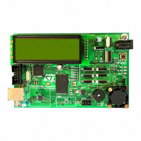
Manufacturer Part Number
STEVAL-IFS003V1
Description
BOARD STLM75/STDS75/ST72F651
Manufacturer
STMicroelectronics
Datasheets
1.STLM75DS2F.pdf
(40 pages)
2.STDS75M2F.pdf
(39 pages)
3.STEVAL-IFS003V1.pdf
(161 pages)
4.STEVAL-IFS003V1.pdf
(4 pages)
Specifications of STEVAL-IFS003V1
Design Resources
STEVAL-IFS003V1 Gerber Files STEVAL-IFS003V1 Schematic STEVAL-IFS003V1 Bill of Materials
Sensor Type
Temperature
Sensing Range
-55°C ~ 125°C
Interface
I²C
Voltage - Supply
7.5 V ~ 19 V
Embedded
Yes, MCU, 8-Bit
Utilized Ic / Part
ST72F651, STDS75, STLM75
Silicon Manufacturer
ST Micro
Silicon Core Number
STLM75/STDS75 And ST72F651AR6
Kit Application Type
Sensing - Temperature
Application Sub Type
Temperature Sensor
Kit Contents
Board
Lead Free Status / RoHS Status
Lead free / RoHS Compliant
Sensitivity
-
Lead Free Status / Rohs Status
Lead free / RoHS Compliant
Other names
497-6238


Functional description
3.3
Note:
3.4
3.4.1
3.4.2
3.4.3
20/40
Serial interface
Writing to and reading from the STLM75 registers is accomplished via the two-wire serial
interface protocol which requires that one device on the bus initiates and controls all READ
and WRITE operations. This device is called the “master” device. The master device also
generates the SCL signal which provides the clock signal for all other devices on the bus.
These other devices on the bus are called “slave” devices. The STLM75 is a slave device
(see
During operations, one data bit is transmitted per clock cycle. All operations follow a
repeating, nine-clock-cycle pattern that consists of eight bits (one byte) of transmitted data
followed by an acknowledge (ACK) or not acknowledge (NACK) from the receiving device.
There are no unused clock cycles during any operation, so there must not be any breaks in
the data stream and ACKs/NACKs during data transfers. Consequently, having too few
clock cycles can lead to incorrect operation if an inadvertent 8-bit READ from a 16-bit
register occurs. So, the entire word must be transferred out regardless of the superflous
trailing zeroes.
Table 9.
2-wire bus characteristics
The bus is intended for communication between different ICs. It consists of two lines: a bi-
directional data signal (SDA) and a clock signal (SCL). Both the SDA and SCL lines must be
connected to a positive supply voltage via a pull-up resistor.
The following protocol has been defined:
●
●
●
Accordingly, the following bus conditions have been defined (see
Bus not busy
Both data and clock lines remain high.
Start data transfer
A change in the state of the data line, from high to low, while the clock is high, defines the
START condition.
Stop data transfer
A change in the state of the data line, from low to high, while the clock is high, defines the
STOP condition.
MSB
Bit7
Data transfer may be initiated only when the bus is not busy.
During data transfer, the data line must remain stable whenever the clock line is high.
Changes in the data line, while the clock line is high, will be interpreted as control
signals.
Table
1
9). Both the master and slave devices can send and receive data on the bus.
STLM75 serial bus slave addresses
Bit6
0
Bit5
0
Doc ID 13296 Rev 12
Bit4
1
Bit3
A2
Bit2
A1
Figure 6 on page
Bit1
A0
STLM75
21):
R/W
Bit0
LSB
Related parts for STEVAL-IFS003V1
Image
Part Number
Description
Manufacturer
Datasheet
Request
R

Part Number:
Description:
BOARD EVAL SPZB260 MOD FOR STR9
Manufacturer:
STMicroelectronics
Datasheet:

Part Number:
Description:
BOARD EVAL EXTENSION SN250
Manufacturer:
STMicroelectronics
Datasheet:

Part Number:
Description:
BOARD EVAL AB-54003L-512
Manufacturer:
STMicroelectronics
Datasheet:

Part Number:
Description:
BOARD REF DESIGN RF DMOS PWR AMP
Manufacturer:
STMicroelectronics
Datasheet:

Part Number:
Description:
BOARD EVAL PWR AMP AB-84008L-470
Manufacturer:
STMicroelectronics
Datasheet:

Part Number:
Description:
BOARD EVAL FOR STM32F103XX
Manufacturer:
STMicroelectronics
Datasheet:

Part Number:
Description:
BOARD EVAL AB-54003L-512
Manufacturer:
STMicroelectronics
Datasheet:

Part Number:
Description:
BOARD SMART PLUG STM32 SPZB260PR
Manufacturer:
STMicroelectronics
Datasheet:

Part Number:
Description:
BOARD DEMO BLUETOOTH SPBT2532C2
Manufacturer:
STMicroelectronics
Datasheet:
Part Number:
Description:
ZIGBEE USB DONGLE EVAL KIT
Manufacturer:
STMicroelectronics
Datasheet:
Part Number:
Description:
STMicroelectronics [RIPPLE-CARRY BINARY COUNTER/DIVIDERS]
Manufacturer:
STMicroelectronics
Datasheet:
Part Number:
Description:
STMicroelectronics [LIQUID-CRYSTAL DISPLAY DRIVERS]
Manufacturer:
STMicroelectronics
Datasheet:

Part Number:
Description:
BOARD EVAL FOR MEMS SENSORS
Manufacturer:
STMicroelectronics
Datasheet: