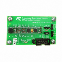
STEVAL-IFS006V1 STMicroelectronics, STEVAL-IFS006V1 Datasheet

STEVAL-IFS006V1
Specifications of STEVAL-IFS006V1
STEVAL-IFS006V1
Available stocks
Related parts for STEVAL-IFS006V1
STEVAL-IFS006V1 Summary of contents
Page 1
Features ■ Low side or high side switch configuration ■ supply voltage range ■ Overload and short circuit protections ■ Internal voltage clamping ■ Supply and output reversal protection ■ Thermal shutdown ■ GND and ...
Page 2
Contents Contents 1 Block and pin connection diagrams . . . . . . . . . . . . . . . . . . . . . . . . . . . . 3 2 Electrical specifications ...
Page 3
TDE1708DFT 1 Block and pin connection diagrams Figure 1. Block diagram Block and pin connection diagrams 3/14 ...
Page 4
Block and pin connection diagrams Figure 2. Pin connection diagram (top view) Table 2. Pin functions o Pin Note: Lead frame can be connected to ground. 4/14 Function Led driver High ...
Page 5
TDE1708DFT 2 Electrical specifications 2.1 Thermal data Table 3. Thermal data Symbol R Thermal resistance junction-ambient. (max) thJA R Thermal resistance junction-case. (max) thJC 1. Soldered layer board with 4 vias in the pad. 2.2 Absolute maximum ...
Page 6
Electrical specifications 2.3 Electrical characteristics Table 5. Electrical characteristics ( +85 °C unless otherwise specified Symbol Parameter V Supply voltage s I Supply reverse current sr I Quiescent current q ...
Page 7
TDE1708DFT 2.4 Dynamic information Table 6. Dynamic information (V Symbol Parameter t Propagation turn on time on t Propagation turn off time off Delayed turn on time / nF t don delay capacitor Minimum delayed min ...
Page 8
Application information 3 Application information The LED driver tells the output status. It can source or sink current (I according to the output configuration chosen. The thresholds, represented by the output comparator in the block diagram, are set at about ...
Page 9
TDE1708DFT 3.1 Adjustable input hysteresis circuit The TDE1708DFT is a device realized in bipolar technology and therefore it has the usual problems of temperature compensation that such technology involves; despite all it maintains an input dynamics within 1 V over ...
Page 10
Package mechanical data 4 Package mechanical data In order to meet environmental requirements, ST offers these devices in different grades of ® ECOPACK packages, depending on their level of environmental compliance. ECOPACK specifications, grade definitions and product status are available ...
Page 11
TDE1708DFT 4.2 DFN (4x4) mechanical data and package dimensions Table 7. Package dimensions Dim Typ Min 0.90 0.80 0.02 0 0.20 0.30 0.23 4 3.90 3 2.82 4 3.90 ...
Page 12
Package mechanical data Figure 7. Package dimension Top view 12/14 Bottom view Sitting plane TDE1708DFT ...
Page 13
TDE1708DFT 5 Revision history Figure 8. Document revision history Date 26-Jun-2006 31-Oct-2006 09-Jan-2007 27-Feb-2009 Revision 1 Initial release. Updated package in cover page, inserted low/high side Updated I in Table 5 on page SCHS 4 Updated ...
Page 14
... Information in this document is provided solely in connection with ST products. STMicroelectronics NV and its subsidiaries (“ST”) reserve the right to make changes, corrections, modifications or improvements, to this document, and the products and services described herein at any time, without notice. All ST products are sold pursuant to ST’s terms and conditions of sale. ...


