Z8F64200100KITG Zilog, Z8F64200100KITG Datasheet - Page 16
Z8F64200100KITG
Manufacturer Part Number
Z8F64200100KITG
Description
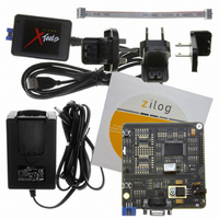
KIT DEV FOR Z8 ENCORE 16K TO 64K
Manufacturer
Zilog
Series
Z8 Encore!®r
Type
MCUr
Specifications of Z8F64200100KITG
Contents
Hardware, Software and Documentation
Processor To Be Evaluated
Z8F642
Data Bus Width
8 bit
Interface Type
RS-232
Silicon Manufacturer
Zilog
Core Architecture
Z8 Encore
Silicon Core Number
Z8F6423FT020
Silicon Family Name
XP F64XX
Kit Contents
Board Cables CD Power Supply
Rohs Compliant
Yes
For Use With/related Products
Z8F642
For Use With
269-4661 - KIT ACC ETHERNET SMART CABLE
Lead Free Status / RoHS Status
Lead free / RoHS Compliant
Other names
269-4540


Schematics
D
C
B
A
Header 1
Header 1
Header 1
Header 1
Header 1
Header 1
Header 1
VCC_33V
JP13
JP14
JP6
JP7
JP8
JP9
JP10
1
1
1
1
1
1
1
PH0_ANA8
GND
GND
PF7
PF6
PF5
PF4
PF3
PF2
PF1
C26
0.001uF
VCC_33V
PH1_ANA9
5
SW2
5
1
C27
0.001uF
L1
IO
PB0_ANA0
RESET
-RESET
EMI Filter
IO
3
AGND
C28
0.001uF
C15
0.001uF
C19
0.001uF
PB1_ANA1
AVDD
R12
220
C23
18pF
R13 100K
PA0_T0IN
Y1
18.432MHz
C16
C20
C29
0.001uF
0.1uF
0.1uF
PB4_ANA4
PH3_ANA11
Figure 4. Z8 Encore! XP F64XX Series Development Board (Continued)
PH2_ANA10
PH0_ANA8
PH1_ANA9
PB0_ANA0
PB1_ANA1
PB4_ANA4
PB5_ANA5
PB6_ANA6
PB7_ANA7
PB3_ANA3
PB2_ANA2
VREF
XOUT
PA0_T0IN
PD1_T3OUT
PD0_T3IN
XIN
18pF
C24
C30
0.001uF
PD2
PC2_SS
PF6
PF5
PF4
PF3
PE4
PE3
PE2
PE1
PE0
PF2
PF1
PF0
PB5_ANA5
C11
0.001uF
VCC_33V
VCC_33V
PA2
PA1_T0OUT
GND
GND
J2
25
23
21
19
17
15
13
11
9
7
5
3
1
4
4
10
11
12
13
14
15
16
17
18
19
20
21
22
23
24
C12
1
2
3
4
5
6
7
8
9
0.1uF
PB6_ANA6
C31
0.001uF
26
24
22
20
18
16
14
12
10
8
6
4
2
U6
PA0/T0IN
PD2
PC2/SS
PF6
RESET
VDD
PF5
PF4
PF3
PE4
PE3
GND
PE2
PE1
PE0
GND
PF2
PF1
PF0
VDD
PD1/T3OUT
PD0/T3IN
XOUT
XIN
PB7_ANA7
C32
0.001uF
PB3_ANA3
C33
0.001uF
PD7/RCOUT
PC7/T2OUT
PC1/T1OUT
PD6/CTS1
PC6/T2IN
PC0/T1IN
PA7/SDA
PC3/SCK
PB2_ANA2
C34
0.001uF
GND
VDD
VDD
DBG
GND
PG0
PG1
PG2
PE5
PE6
PE7
PG3
PG4
PG5
PG6
PG7
Z8F642
64
63
62
61
60
59
58
57
56
55
54
53
52
51
50
49
48
47
46
45
44
43
42
41
C35
0.001uF
PH2_ANA10
PD7_RCOUT
VCC_33V
VCC_33V
3
PA7_SDA
PD6_CTS1
PC3_SCK
GND
PC7_T2OUT
PC1_T1OUT
GND
3
C13
0.1uF
PC6_T2IN
PC0_T1IN
PG0
PG1
PG2
PE5
PE6
PE7
PG3
PG4
PG5
PG6
PG7
DBG
C36
0.001uF
PH3_ANA11
C14
0.001uF
C37
0.001uF
AGND
C21
0.1uF
C17
0.1uF
PC0_T1IN
+
C22
0.001uF
C25
22uF
PA5_TXD0
PA3_CTS0
PA4_RXD0
C18
0.001uF
DBG
Z8 Encore! XP
C38
0.01uF
PG1
PG2
PG3
PG4
PG5
PG6
PG7
DBG
PA5_TXD0
PA3_CTS0
PA4_RXD0
2
connector 1
for
reference
only
2
Header 1
Header 1
Header 1
Header 1
Header 1
Header 1
Header 1
JP15
1
JP16
1
JP17
1
JP18
1
JP19
1
JP20
1
JP21
1
®
Title
Size
Date:
F64XX Series Development Kit
B
PE7
PE5
PE3
PE1
VCC_33V
PC4_MOSI
PC7_T2OUT
PC3_SCK
PC0_T1IN
PC1_T1OUT
PD1_T3OUT
PD3
PD5_TXD1
PD7_RCOUT
PF0
PA3_CTS0
PA4_RXD0
PA6_SCL
PA7_SDA
-RESET
VCC_33V
Encore! F642. Evaluation Module. Schematic.
Document Number
VCC_33V
If Module is plugged onto the Dev Platform the local
RS232 interface is disabled by pin 50 of JP2
Friday, June 06, 2003
GND
GND
GND
GND
-TRSTN
NC
NC
NC
NC
NC
NC
-CS2
GND
A21
A22
-CS0
-BUSACK
-F91_WE
connector 2
A6
A10
A8
A13
A15
A18
A19
A2
A11
A4
A5
D1
D3
D5
D7
-MREQ
-WR
96C0918-001
11
13
15
17
19
21
23
25
27
29
31
33
35
37
39
41
43
45
47
49
51
53
55
57
59
1
3
5
7
9
JP2
HEADER 30x2/SM
11
13
15
17
19
21
23
25
27
29
31
33
35
37
39
41
43
45
47
49
51
53
55
57
59
1
3
5
7
9
JP1
HEADER 30x2/SM
2
4
6
8
10
12
14
16
18
20
22
24
26
28
30
32
34
36
38
40
42
44
46
48
50
52
54
56
58
60
Sheet
2
4
6
8
10
12
14
16
18
20
22
24
26
28
30
32
34
36
38
40
42
44
46
48
50
52
54
56
58
60
1
1
UM015110-0508
NC
NC
NC
NC
NC
NC
NC
-DIS_IrDA
User Manual
GND
PC5_MISO
PC6_T2IN
PA1_T0OUT
PD6_CTS1
PD4_RXD1
PD0_T3IN
PA5_TXD0
-DIS_FLASH
A0
A3
A14
A16
A23
-CS1
GND
A7
A9
A17
D0
D2
D4
D6
-IOREQ
-RD
-INSTRD
-BUSREQ
PC2_SS
PA0_T0IN
PA2
GND
VCC_33V
VCC_33V
GND
A1
A12
A20
VCC_33V
PD2
PG0
GND
2
PE6
PE4
PE2
PE0
GND
of
VCC_33V
-DIS_232
-DIS_IRDA
2
Rev
A
D
C
B
A
13
Related parts for Z8F64200100KITG
Image
Part Number
Description
Manufacturer
Datasheet
Request
R

Part Number:
Description:
Communication Controllers, ZILOG INTELLIGENT PERIPHERAL CONTROLLER (ZIP)
Manufacturer:
Zilog, Inc.
Datasheet:

Part Number:
Description:
KIT DEV Z8 ENCORE XP 28-PIN
Manufacturer:
Zilog
Datasheet:

Part Number:
Description:
DEV KIT FOR Z8 ENCORE 8K/4K
Manufacturer:
Zilog
Datasheet:

Part Number:
Description:
KIT DEV Z8 ENCORE XP 28-PIN
Manufacturer:
Zilog
Datasheet:

Part Number:
Description:
DEV KIT FOR Z8 ENCORE 4K TO 8K
Manufacturer:
Zilog
Datasheet:
Part Number:
Description:
CMOS Z8 microcontroller. ROM 16 Kbytes, RAM 256 bytes, speed 16 MHz, 32 lines I/O, 3.0V to 5.5V
Manufacturer:
Zilog, Inc.
Datasheet:
Part Number:
Description:
Low-cost microcontroller. 512 bytes ROM, 61 bytes RAM, 8 MHz
Manufacturer:
Zilog, Inc.
Datasheet:
Part Number:
Description:
Z8 4K OTP Microcontroller
Manufacturer:
Zilog, Inc.
Datasheet:
Part Number:
Description:
CMOS SUPER8 ROMLESS MCU
Manufacturer:
Zilog, Inc.
Datasheet:
Part Number:
Description:
SL1866 CMOSZ8 OTP Microcontroller
Manufacturer:
Zilog, Inc.
Datasheet:
Part Number:
Description:
SL1866 CMOSZ8 OTP Microcontroller
Manufacturer:
Zilog, Inc.
Datasheet:
Part Number:
Description:
OTP (KB) = 1, RAM = 125, Speed = 12, I/O = 14, 8-bit Timers = 2, Comm Interfaces Other Features = Por, LV Protect, Voltage = 4.5-5.5V
Manufacturer:
Zilog, Inc.
Datasheet:
Part Number:
Description:
Manufacturer:
Zilog, Inc.
Datasheet: