R0K561622S000BE Renesas Electronics America, R0K561622S000BE Datasheet - Page 398
R0K561622S000BE
Manufacturer Part Number
R0K561622S000BE
Description
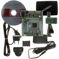
KIT STARTER FOR H8SX/1622
Manufacturer
Renesas Electronics America
Series
Renesas Starter Kits (RSK)r
Type
MCUr
Specifications of R0K561622S000BE
Contents
Board, Cables, CD, Debugger, Power Supply
Silicon Manufacturer
Renesas
Features
Coding And Debugging, E10A Emulator, RS232 Serial Connection
Kit Contents
Board
Silicon Family Name
H8SX/1622F
Silicon Core Number
R5F61622N50LGV
Lead Free Status / RoHS Status
Lead free / RoHS Compliant
For Use With/related Products
H8SX/1622
Lead Free Status / RoHS Status
Lead free / RoHS Compliant, Lead free / RoHS Compliant


Section 10 Data Transfer Controller (DTC)
Table 10.10 Number of Cycles Required for Each Execution State
[Legend]
m: Number of wait cycles 0 to 7 (For details, see section 8, Bus Controller (BSC).)
The number of execution cycles is calculated from the formula below. Note that Σ means the sum
of all transfers activated by one activation event (the number in which the CHNE bit is set to 1,
plus 1).
10.5.10 DTC Bus Release Timing
The DTC requests the bus mastership to the bus arbiter when an activation request occurs. The
DTC releases the bus after a vector read, transfer information read, a single data transfer, or
transfer information writeback. The DTC does not release the bus during transfer information
read, single data transfer, or transfer information writeback.
10.5.11 DTC Priority Level Control to the CPU
The priority of the DTC activation sources over the CPU can be controlled by the CPU priority
level specified by bits CPUP2 to CPUP0 in CPUPCR and the DTC priority level specified by bits
DTCP2 to DTCP0. For details, see section 6, Interrupt Controller.
Rev. 2.00 Sep. 16, 2009 Page 368 of 1036
REJ09B0414-0200
Object to be Accessed
Bus width
Access cycles
Execution
status
Number of execution cycles = I
Vector read S
Transfer information read S
Transfer information write S
Byte data read S
Word data read S
Longword data read S
Byte data write S
Word data write S
Longword data write S
Internal operation S
I
L
M
L
M
N
L
M
J
k
On-Chip
RAM
32
1
1
1
1
1
1
1
1
1
1
•
S
I
On-Chip
ROM
32
1
1
1
1
1
1
1
1
1
1
+ Σ (J
•
8
2
2
4
8
2
4
8
S
On-Chip I/O
J
Registers
+ K
16
2
2
2
4
2
2
4
•
S
32
2
2
2
2
2
2
2
K
+ L
1
•
2
8
8
8
2
4
8
2
4
8
S
L
+ M
8
3
12 + 4m
12 + 4m
12 + 4m
3 + m
4 + 2m
12 + 4m
3 + m
4 + 2m
12 + 4m
External Devices
•
S
M
) + N
2
4
4
4
2
2
4
2
2
4
•
S
16
N
3
6 + 2m
6 + 2m
6 + 2m
3 + m
3 + m
6 + 2m
3 + m
3 + m
6 + 2m
Related parts for R0K561622S000BE
Image
Part Number
Description
Manufacturer
Datasheet
Request
R

Part Number:
Description:
KIT STARTER FOR M16C/29
Manufacturer:
Renesas Electronics America
Datasheet:

Part Number:
Description:
KIT STARTER FOR R8C/2D
Manufacturer:
Renesas Electronics America
Datasheet:

Part Number:
Description:
R0K33062P STARTER KIT
Manufacturer:
Renesas Electronics America
Datasheet:

Part Number:
Description:
KIT STARTER FOR R8C/23 E8A
Manufacturer:
Renesas Electronics America
Datasheet:

Part Number:
Description:
KIT STARTER FOR R8C/25
Manufacturer:
Renesas Electronics America
Datasheet:

Part Number:
Description:
KIT STARTER H8S2456 SHARPE DSPLY
Manufacturer:
Renesas Electronics America
Datasheet:

Part Number:
Description:
KIT STARTER FOR R8C38C
Manufacturer:
Renesas Electronics America
Datasheet:

Part Number:
Description:
KIT STARTER FOR R8C35C
Manufacturer:
Renesas Electronics America
Datasheet:

Part Number:
Description:
KIT STARTER FOR R8CL3AC+LCD APPS
Manufacturer:
Renesas Electronics America
Datasheet:
Part Number:
Description:
KIT STARTER FOR RX610
Manufacturer:
Renesas Electronics America
Datasheet:

Part Number:
Description:
KIT STARTER FOR R32C/118
Manufacturer:
Renesas Electronics America
Datasheet:

Part Number:
Description:
KIT DEV RSK-R8C/26-29
Manufacturer:
Renesas Electronics America
Datasheet:

Part Number:
Description:
KIT STARTER FOR SH7124
Manufacturer:
Renesas Electronics America
Datasheet:

Part Number:
Description:
KIT DEV FOR SH7203
Manufacturer:
Renesas Electronics America
Datasheet:
Part Number:
Description:
KIT STARTER FOR R8C/18191A1B
Manufacturer:
Renesas Electronics America
Datasheet: