EVAL-AD7655CB Analog Devices Inc, EVAL-AD7655CB Datasheet
EVAL-AD7655CB
Specifications of EVAL-AD7655CB


Related parts for EVAL-AD7655CB


EVAL-AD7655CB Summary of contents
Page 1
FEATURES 4-channel, 16-bit resolution ADC 2 track-and-hold amplifiers Throughput 1 MSPS (normal mode) 888 kSPS (impulse mode) Analog input voltage range pipeline delay Parallel and serial 5 V/3 V interface SPI®/QSPI™/MICROWIRE™/DSP compatible Single 5 ...
Page 2
... Serial Interface ............................................................................ 20 Master Serial Interface............................................................... 20 Slave Serial Interface .................................................................. 22 Microprocessor Interfacing....................................................... 24 SPI Interface (ADSP-219 Application Hints ........................................................................... 25 Layout .......................................................................................... 25 Evaluating the AD7655 Performance ...................................... 25 Outline Dimensions ....................................................................... 26 Ordering Guide .......................................................................... 27 12/04—Rev Rev. A Changes to Figure 17...................................................................... 15 Changes to Figure 18...................................................................... 16 Changes to Voltage Reference Input section .............................. 17 Changes to Conversion Control section ..................................... 18 Changes to Digital Interface section ...
Page 3
SPECIFICATIONS AVDD = DVDD = 5 V, OVDD = 2 5. Table 2. Parameter RESOLUTION ANALOG INPUT Voltage Range Common-Mode Input Voltage Analog Input CMRR Input Current 1 Input Impedance THROUGHPUT SPEED Complete Cycle (2 Channels) ...
Page 4
AD7655 Parameter POWER SUPPLIES Specified Performance AVDD DVDD OVDD 9 Operating Current AVDD DVDD OVDD Power Dissipation 11 TEMPERATURE RANGE Specified Performance 1 See the Analog Inputs section. 2 Linearity is tested using endpoints, not best fit. 3 LSB means ...
Page 5
TIMING SPECIFICATIONS AVDD = DVDD = 5 V, OVDD = 2 5. Table 3. Parameter CONVERSION AND RESET (See Figure 21 and Figure 22) Convert Pulse Width Time Between Conversions (Normal Mode/Impulse Mode) CNVST Low to ...
Page 6
AD7655 Parameter SLAVE SERIAL INTERFACE MODES (See Figure 31 and Figure 32) External SCLK Setup Time External SCLK Active Edge to SDOUT Delay SDIN Setup Time SDIN Hold Time External SCLK Period External SCLK High External SCLK Low 1 In ...
Page 7
ABSOLUTE MAXIMUM RATINGS Table 5. Parameter Values Analog Input 1 1 INAx , INBx , REFx, INxN, REFGND AVDD + 0 AGND − 0.3 V Ground Voltage Differences AGND, DGND, OGND ±0.3 V Supply Voltages AVDD, DVDD, OVDD ...
Page 8
AD7655 PIN CONFIGURATION AND FUNCTION DESCRIPTIONS Table 6. Pin Function Descriptions Pin No. Mnemonic Type 1 Description 1, 47, 48 AGND P Analog Power Ground Pin. 2 AVDD P Input Analog Power Pin. Nominally Multiplexer ...
Page 9
Pin No. Mnemonic Type Description 15 D[6] DI/O When SER/PAR is LOW, this output is used as Bit 6 of the parallel port data output bus. or INVSCLK When SER/PAR is HIGH, this input, part of the serial port, ...
Page 10
AD7655 1 Pin No. Mnemonic Type Description 35 CNVST DI Start Conversion. A falling edge on CNVST puts the internal sample-and-hold into the hold state and initiates a conversion. In impulse mode (IMPULSE = HIGH), if CNVST is held LOW ...
Page 11
TERMINOLOGY Integral Nonlinearity Error (INL) Linearity error refers to the deviation of each individual code from a line drawn from negative full scale through positive full scale. The point used as negative full scale occurs ½ LSB before the first ...
Page 12
AD7655 TYPICAL PERFORMANCE CHARACTERISTICS –1 –2 –3 –4 –5 32768 0 16384 CODE Figure 5. Integral Nonlinearity vs. Code 8000 7059 6894 7000 6000 5000 4000 3000 2000 1230 1094 1000 ...
Page 13
FREQUENCY (kHz) Figure 11. SNR, SINAD, and ENOB vs. Frequency –75 –80 SFDR –85 CROSSTALK –90 –95 CROSSTALK THD –100 THIRD HARMONIC SECOND HARMONIC ...
Page 14
AD7655 APPLICATION INFORMATION CIRCUIT INFORMATION The AD7655 is a very fast, low power, single-supply, precise simultaneous sampling 16-bit ADC. The AD7655 provides the user with two on-chip, track-and- hold, successive approximation ADCs that do not exhibit any pipeline or latency, ...
Page 15
ANALOG SUPPLY (5V) + 10μF AD780 2.5V REF 1MΩ REF 50kΩ 1μF NOTE 1 100nF NOTE 2 NOTE 3 50Ω - 10Ω NOTE ANALOG INPUT A1 2.7nF C C NOTE 5 50Ω - 10Ω NOTE ...
Page 16
AD7655 TYPICAL CONNECTION DIAGRAM Figure 17 shows a typical connection diagram for the AD7655. Some of the circuitry shown in this diagram is optional and is discussed in the following sections. ANALOG INPUTS Figure 18 shows a simplified analog input ...
Page 17
Table 8. Recommended Driver Amplifiers Amplifier Typical Application ADA4841 Very low noise, low distortion, low power, low frequency AD829 Very low noise, low frequency AD8021 Very low noise, high frequency AD8022 Very low noise, high frequency, dual AD8605/AD8606 ...
Page 18
AD7655 CONVERSION CONTROL Figure 21 shows a detailed timing diagram of the conversion process. The AD7655 is controlled by the signal CNVST , which initiates conversion. Once initiated, it cannot be restarted or aborted, even by the power-down input, PD, ...
Page 19
Slave Parallel Interface In slave parallel reading mode, the data can be read either after each conversion, which is during the next acquisition phase, or during the other channel’s conversion, or during the following conversion, as shown in Figure 24 ...
Page 20
AD7655 SERIAL INTERFACE The AD7655 is configured to use the serial interface when the SER/ PAR is held high. The AD7655 outputs 32 bits of data, MSB first, on the SDOUT pin. The order of the channels being output is ...
Page 21
EXT/INT = 0 CS, RD CNVST BUSY t 3 EOC SYNC SCLK SDOUT Figure 28. Master Serial Data Timing ...
Page 22
AD7655 SLAVE SERIAL INTERFACE External Clock The AD7655 is configured to accept an externally supplied serial data clock on the SCLK pin when the EXT/ INT pin is held high. In this mode, several methods can be used to read ...
Page 23
EXT/INT = 1 CS EOC BUSY SCLK SDOUT X D15 D14 SDIN D15 ...
Page 24
AD7655 MICROPROCESSOR INTERFACING The AD7655 is ideally suited for traditional dc measurement applications supporting a microprocessor and for ac signal processing applications interfacing to a digital signal processor. The AD7655 is designed to interface with either a parallel 8-bit-wide or ...
Page 25
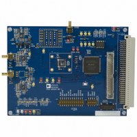
... OGND is connected to the digital system ground. EVALUATING THE AD7655 PERFORMANCE A recommended layout for the AD7655 is outlined in the EVAL-AD7655CB evaluation board documentation. The evaluation board package includes a fully assembled and tested evaluation board, documentation, and software for controlling the board from a PC via the EVAL-CONTROL-BRD3. ...
Page 26
AD7655 OUTLINE DIMENSIONS 1.45 1.40 1.35 0.15 0.05 ROTATED 90° CCW BSC SQ PIN 1 INDICATOR 1.00 12° MAX 0.85 0.80 SEATING PLANE 0.75 1.60 0.60 MAX 0.45 0.20 0.09 7° 3.5° 12 0° SEATING 0.08 MAX PLANE VIEW A ...
Page 27
... AD7655ASTZ −40°C to +85°C AD7655ASTZRL 1 −40°C to +85°C 2 EVAL-AD7655CB 3 EVAL-CONTROL-BRD3 Pb-free part. 2 This board can be used as a standalone evaluation board or in conjunction with the EVAL-CONTROL-BRD3 for evaluation/demonstration purposes. 3 This board allows control and communicate with all Analog Devices evaluation boards ending in CB designators. ...
Page 28
AD7655 NOTES © 2005 Analog Devices, Inc. All rights reserved. Trademarks and registered trademarks are the property of their respective owners. C03536-0-9/05(B) T Rev Page ...