AD9549/PCBZ Analog Devices Inc, AD9549/PCBZ Datasheet - Page 10
AD9549/PCBZ
Manufacturer Part Number
AD9549/PCBZ
Description
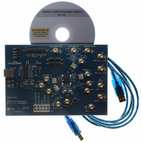
BOARD EVALUATION FOR AD9549
Manufacturer
Analog Devices Inc
Datasheet
1.AD9549ABCPZ.pdf
(76 pages)
Specifications of AD9549/PCBZ
Main Purpose
Timing, Clock Generator
Embedded
No
Utilized Ic / Part
AD9549
Primary Attributes
2 Inputs, 2 Outputs, VCO
Secondary Attributes
CMOS, HSTL Output Logic, Graphical User Interface
Lead Free Status / RoHS Status
Lead free / RoHS Compliant


AD9549
PIN CONFIGURATION AND FUNCTION DESCRIPTIONS
Table 5. Pin Function Descriptions
Pin No.
1
2, 4, 6, 8
3, 5, 7
9, 10, 54, 55
11, 19, 23 to
26, 29, 30, 36,
42, 44, 45, 53
12
13
14, 46, 47, 49
15
16
17, 18
Input/
Output
I
I
I
I/O
I
I
I
I
I
I
Pin Type
Power
Power
Power
3.3 V CMOS
Power
Differential
input
Differential
input
Power
Differential
input
Differential
input
REFA_INB
REFB_INB
NOTES
1. NC = NO CONNECT.
2. THE EXPOSED THERMAL DIE ON THE BOTTOM OF THE PACKAGE PROVIDES
DVDD_I/O
REFA_IN
REFB_IN
THE ANALOG GROUND FOR THE PART. THIS EXPOSED PAD MUST BE
CONNECTED TO GROUND FOR PROPER OPERATION.
AVDD3
DVDD
DVDD
DVDD
AVDD
DVSS
DVSS
DVSS
DVSS
S1
S2
Mnemonic
DVDD_I/O
DVSS
DVDD
S1, S2, S3, S4
AVDD
REFA_IN
REFA_INB
AVDD3
REFB_IN
REFB_INB
NC
10
11
12
13
14
15
16
1
2
3
4
5
6
7
8
9
PIN 1
INDICATOR
Figure 2. Pin Configuration
Rev. D | Page 10 of 76
Description
I/O Digital Supply.
Digital Ground. Connect to ground.
Digital Supply.
Configurable I/O Pins. These pins are configured under program control (see
the Status and Warnings section) and do not have internal pull-up/pull-down
resistors.
Analog Supply. Connect to a nominal 1.8 V supply.
Frequency/Phase Reference A Input. This internally biased input is typically
ac-coupled and, when configured as such, can accept any differential signal
with single-ended swing between 0.4 V and 3.3 V. If dc-coupled, LVPECL or
CMOS input is preferred.
Complementary Frequency/Phase Reference A Input. Complementary signal
to the input provided on Pin 12. If using a single-ended, dc-coupled CMOS
signal into REFA_IN, bypass this pin to ground with a 0.01 μF capacitor.
Analog Supply. Connect to a nominal 3.3 V supply.
Frequency/Phase Reference B Input. This internally biased input is typically
ac-coupled and, when configured as such, can accept any differential signal
with single-ended swing between 0.4 V and 3.3 V. If dc-coupled, LVPECL or
CMOS input is preferred.
Complementary Frequency/Phase Reference B Input. Complementary signal
to the input provided on Pin 15. If using a single-ended, dc-coupled CMOS
signal into REFB_IN, bypass this pin to ground with a 0.01 μF capacitor.
No Connect. These are excess, unused pins that can be left floating.
(Not to Scale)
AD9549
TOP VIEW
48
47
46
45
44
43
42
41
40
39
38
37
36
35
34
33
DAC_RSET
AVDD3
AVDD3
AVDD
AVDD
AVSS
AVDD
FDBK_IN
FDBK_INB
AVSS
OUT_CMOS
AVDD3
AVDD
OUT
OUTB
AVSS
Related parts for AD9549/PCBZ
Image
Part Number
Description
Manufacturer
Datasheet
Request
R


Part Number:
Description:
±1.7g Dual-Axis IMEMS Accelerometer Evaluation Board
Manufacturer:
Analog Devices Inc
Datasheet:

Part Number:
Description:
Inertial Sensor Evaluation System
Manufacturer:
Analog Devices Inc
Datasheet:
Part Number:
Description:
Manufacturer:
Analog Devices Inc
Datasheet:
Part Number:
Description:
Manufacturer:
Analog Devices Inc
Datasheet:
Part Number:
Description:
Manufacturer:
Analog Devices Inc
Datasheet:
Part Number:
Description:
Manufacturer:
Analog Devices Inc
Datasheet:
Part Number:
Description:
Manufacturer:
Analog Devices Inc
Datasheet:
Part Number:
Description:
Manufacturer:
Analog Devices Inc
Datasheet:
Part Number:
Description:
Manufacturer:
Analog Devices Inc
Datasheet:
Part Number:
Description:
Manufacturer:
Analog Devices Inc
Datasheet:
Part Number:
Description:
Manufacturer:
Analog Devices Inc
Datasheet:
Part Number:
Description:
Manufacturer:
Analog Devices Inc
Datasheet: