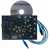
AD9549/PCBZ Analog Devices Inc, AD9549/PCBZ Datasheet - Page 17
AD9549/PCBZ
Manufacturer Part Number
AD9549/PCBZ
Description
BOARD EVALUATION FOR AD9549
Manufacturer
Analog Devices Inc
Datasheet
1.AD9549ABCPZ.pdf
(76 pages)
Specifications of AD9549/PCBZ
Main Purpose
Timing, Clock Generator
Embedded
No
Utilized Ic / Part
AD9549
Primary Attributes
2 Inputs, 2 Outputs, VCO
Secondary Attributes
CMOS, HSTL Output Logic, Graphical User Interface
Lead Free Status / RoHS Status
Lead free / RoHS Compliant


THEORY OF OPERATION
OVERVIEW
The AD9549 provides a clocking output that is directly related
in phase and frequency to the selected (active) reference (REFA
or REFB) but has a phase noise spectrum primarily governed
by the system clock. A wide band of reference frequencies is
supported. Jitter existing on the active reference is greatly reduced
by a programmable digital filter in the digital phase-locked loop
(PLL), which is the core of this product. The AD9549 supports
both manual and automatic holdover. While in holdover, the
AD9549 continues to provide an output as long as the system
clock is maintained. The frequency of the output during hold-
over is an average of the steady state output frequency prior to
holdover.
Also offered are manual and automatic switchover modes for
changing between the two references, should one become suspect
or lost. A digitally controlled oscillator (DCO) is implemented
using a direct digital synthesizer (DDS) with an integrated output
digital-to-analog converter (DAC), clocked by the system clock.
A bypassable PLL-based frequency multiplier is present, enabling
use of an inexpensive, low frequency source for the system clock.
For best jitter performance, the system clock PLL should be
bypassed; and a low noise, high frequency system clock should be
provided directly. Sampling theory sets an upper bound for the
DDS output frequency at 50%
REFSELECT
S1 TO S4
REFA_IN
REFB_IN
OOL AND LOR
MONITOR
IRQ AND
STATUS
INPUT
LOGIC
REF
REF_CNTRL
÷R
LOCK DETECT
PFD
Figure 22. Detailed Block Diagram
FREQ
EST.
INTERFACE
CONTROL
DIGITAL
LOGIC
Rev. D | Page 17 of 76
DIGITAL
FILTER
PROG.
LOOP
HOLDOVER
÷S
SLEW
LIMIT
of f
of 40% of f
of the required off-chip reconstruction filter. The output signal
from the reconstruction filter is fed back to the AD9549, both
to complete the PLL and to be processed through the output
circuitry. The output circuitry includes HSTL and CMOS output
buffers, as well as a frequency doubler for designs that must
provide frequencies above the Nyquist level of the DDS.
The individual functional blocks are described in the following
sections.
DIGITAL PLL CORE (DPLLC)
The digital phase-locked loop core (DPLLC) includes the
frequency estimation block and the digital phase lock control
block driving the DDS.
The start of the DPLLC signal chain is the reference signal, f
which appears on REFA or REFB inputs. The frequency of this
signal can be divided by an integer factor of R via the feedforward
divider. The output of the feedforward divider is routed to the
phase/frequency detector (PFD). Therefore, the frequency at
the input to the PFD is given by
S
HOLDOVER
(where f
f
DIGITAL PLL CORE
PFD
FREQUENCY
2×
TUNING
WORD
S
=
is generally recommended to allow for the selectivity
S
f
R
is the DAC sample rate), but a practical limitation
SYSCLK PORT
R
DDS/DAC
SYSCLK
MULTIPLIER
LOW NOISE
CLOCK
AMP
OUT_CMOS
OUT
FDBK_IN
DAC_OUT
EXTERNAL
LOW-PASS
ANALOG
FILTER
AD9549
R
,
Related parts for AD9549/PCBZ
Image
Part Number
Description
Manufacturer
Datasheet
Request
R


Part Number:
Description:
±1.7g Dual-Axis IMEMS Accelerometer Evaluation Board
Manufacturer:
Analog Devices Inc
Datasheet:

Part Number:
Description:
Inertial Sensor Evaluation System
Manufacturer:
Analog Devices Inc
Datasheet:
Part Number:
Description:
Manufacturer:
Analog Devices Inc
Datasheet:
Part Number:
Description:
Manufacturer:
Analog Devices Inc
Datasheet:
Part Number:
Description:
Manufacturer:
Analog Devices Inc
Datasheet:
Part Number:
Description:
Manufacturer:
Analog Devices Inc
Datasheet:
Part Number:
Description:
Manufacturer:
Analog Devices Inc
Datasheet:
Part Number:
Description:
Manufacturer:
Analog Devices Inc
Datasheet:
Part Number:
Description:
Manufacturer:
Analog Devices Inc
Datasheet:
Part Number:
Description:
Manufacturer:
Analog Devices Inc
Datasheet:
Part Number:
Description:
Manufacturer:
Analog Devices Inc
Datasheet:
Part Number:
Description:
Manufacturer:
Analog Devices Inc
Datasheet: