AD9549/PCBZ Analog Devices Inc, AD9549/PCBZ Datasheet - Page 19
AD9549/PCBZ
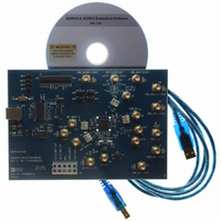
Manufacturer Part Number
AD9549/PCBZ
Description
BOARD EVALUATION FOR AD9549
Manufacturer
Analog Devices Inc
Datasheet
1.AD9549ABCPZ.pdf
(76 pages)
Specifications of AD9549/PCBZ
Main Purpose
Timing, Clock Generator
Embedded
No
Utilized Ic / Part
AD9549
Primary Attributes
2 Inputs, 2 Outputs, VCO
Secondary Attributes
CMOS, HSTL Output Logic, Graphical User Interface
Lead Free Status / RoHS Status
Lead free / RoHS Compliant


The DCO has a minimum frequency, f
Output Characteristics section of the AC Specifications table).
This minimum frequency imposes a lower bound, S
feedback divider value, as well.
Note that reduced DCO frequencies result in worse jitter
performance (a consequence of the reduced slew rate of the
sinusoid generated by the DDS).
Forward and Reverse FEC Clock Scaling
The feedforward divider (divide-by-R) and feedback divider
(divide-by-S) enable FEC clock scaling. For instance, to multiply
the incoming signal by 255/237, set the S-divider to 255 and the
R-divider to 237. Be careful to abide by the limitations on the R-
and S-dividers, and make sure the phase detector input frequency
is within specified limits.
Phase Detector
The phase detector is composed of two detectors: a coarse phase
detector and a fine phase detector. The two detectors operate in
parallel. Both detectors measure the duration (Δt) of the pulses
generated by a conventional three-state phase/frequency detector.
Together, the fine and coarse phase detectors produce a digital
word that is a time-to-digital conversion of the separation
between the edge transitions of the prescaled reference signal
and the feedback signal.
If the fine phase detector is able to produce a valid result, this
result alone serves as the phase error measurement. If the fine
phase detector is in either an overflow or underflow condition,
the phase error measurement uses the coarse phase detector
instead.
Digital Loop Filter
The digital loop filter integrates and low-pass filters the digital
phase error values delivered by the phase detector. The loop
filter response mimics that of a second-order RC network used
to filter the output of a typical phase detector and charge pump
combination, as shown in Figure 24.
The building blocks implemented on the AD9549, however, are
digital. A time-to-digital converter that produces digital values
proportional to the edge timing error between the CLK and
feedback signals replaces the phase-frequency detector and
charge pump. A digital filter that processes the edge timing
S
CLK
MIN
=
max
Figure 24. Typical Analog PLL Block Diagram
FREQUENCY
DETECTOR
PHASE/
R
f
DCO
CHANGE
f
[
R
PUMP
MIN
]
1 ,
LOOP FILTER
DCO[MIN]
C1
R2
C2
(see the DAC
VCO
MIN
, on the
Rev. D | Page 19 of 76
error samples from the time-to-digital converter replaces the loop
filter. A DDS replaces the VCO, which produces a frequency that
is linearly related to the digital value provided by the loop filter.
This is shown in Figure 25 with some additional detail.
The samples provided by the time-to-digital converter are delivered
to the loop filter at a sample rate equal to the CLK frequency (that
is, f
digital converter output at a rate determined by the P-divider.
The value of P is programmable via the I/O register map. It is
stored as a 5-bit number, P
the equation
where 5 ≤ P
Hence, the P-divider can provide divide ratios between 32 and
65,536 in power-of-2 steps. With a DAC sample rate of 1 GHz,
the loop filter sample rate can range from as low as 15.26 kHz to
a maximum of 31.25 MHz. Coupled to the loop filter is a cascaded
comb integrator (CCI) filter that provides a sample rate translation
between the loop filter sample rate (f
rate, f
The choice of P is important because it controls both the
response of the CCI filter and the sample rate of the loop filter.
To understand the method for determining a useful value for P,
it is first necessary to examine the transfer function of the CCI
filter.
or
To evaluate the response in terms of absolute frequency, make
the substitution
where f
H
Analysis of this function reveals that the CCI magnitude response
follows a low-pass characteristic that consists of a series of P lobes.
The lobes are bounded by null points occurring at frequency mul-
tiples of f
predecessor over the frequency range between dc and one-half f
For frequencies greater than one-half f
about the vertical at one-half f
appears between dc and f
response. That is, the magnitude is unity at dc, and it steadily
decreases with frequency until it vanishes at the first null point
(f
S
CCI
/P).
R
/R). The loop filter is intended to oversample the time-to-
P = 2
is to be evaluated.
ω
H
H
S
.
(
S
CCI
=
ω
is the DAC sample rate, and f is the frequency at which
S
)
/P. The peak of each successive lobe is lower than its
PIO
2
CCI
(
f
ω
π
IO
S
f
)
≤ 16.
=
=
P
p
1
1
2
1 (
−
−
1
e
1
e
S
−
jω
/P) exhibits a monotonically decreasing
−
− jω
P
, 1
cos(
IO
cos(
. The value of P
S
. Furthermore, the first lobe (which
2
ωP
ω
)
)
,
S
S
, the response is a reflection
/P) and the DDS sample
ω
ω
=
>
0
0
IO
is related to P by
AD9549
S
.
Related parts for AD9549/PCBZ
Image
Part Number
Description
Manufacturer
Datasheet
Request
R


Part Number:
Description:
±1.7g Dual-Axis IMEMS Accelerometer Evaluation Board
Manufacturer:
Analog Devices Inc
Datasheet:

Part Number:
Description:
Inertial Sensor Evaluation System
Manufacturer:
Analog Devices Inc
Datasheet:
Part Number:
Description:
Manufacturer:
Analog Devices Inc
Datasheet:
Part Number:
Description:
Manufacturer:
Analog Devices Inc
Datasheet:
Part Number:
Description:
Manufacturer:
Analog Devices Inc
Datasheet:
Part Number:
Description:
Manufacturer:
Analog Devices Inc
Datasheet:
Part Number:
Description:
Manufacturer:
Analog Devices Inc
Datasheet:
Part Number:
Description:
Manufacturer:
Analog Devices Inc
Datasheet:
Part Number:
Description:
Manufacturer:
Analog Devices Inc
Datasheet:
Part Number:
Description:
Manufacturer:
Analog Devices Inc
Datasheet:
Part Number:
Description:
Manufacturer:
Analog Devices Inc
Datasheet:
Part Number:
Description:
Manufacturer:
Analog Devices Inc
Datasheet: