AD9549/PCBZ Analog Devices Inc, AD9549/PCBZ Datasheet - Page 39
AD9549/PCBZ
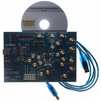
Manufacturer Part Number
AD9549/PCBZ
Description
BOARD EVALUATION FOR AD9549
Manufacturer
Analog Devices Inc
Datasheet
1.AD9549ABCPZ.pdf
(76 pages)
Specifications of AD9549/PCBZ
Main Purpose
Timing, Clock Generator
Embedded
No
Utilized Ic / Part
AD9549
Primary Attributes
2 Inputs, 2 Outputs, VCO
Secondary Attributes
CMOS, HSTL Output Logic, Graphical User Interface
Lead Free Status / RoHS Status
Lead free / RoHS Compliant


STATUS AND WARNINGS
Status Pins
Four pins (S1 to S4) are reserved for providing device status
information to the external environment. These four pins are
individually programmable (via the serial I/O port) as an OR'ed
combination of six possible status indications. Each pin has a
dedicated group of control register bits that determine which
internal status flags are used to provide an indication on a
particular pin, as shown in Figure 49.
Reference Monitor Status
In the case of reference monitoring status information, a pin
can be programmed for either REFA or REFB, but not both.
In addition, the OR'ed output configuration allows the user to
combine multiple status flags into a single status indication. For
example, if both the LOR and OOL control register bits are true,
the status pin associated with that particular control register
gives an indication if either the LOR or OOL status flag is
asserted for the selected reference (A or B).
FREQUENCY LOCK DETECT
PHASE LOCK DETECT
REFA INVALID
REFB INVALID
REFA LOR
REFA OOL
REFB LOR
REFB OOL
STATUS FLAGS
INTERNAL
IRQ
CONTROL REGISTER
FREQUENCY LOCK
REFAB INVALID
PHASE LOCK
STATUS PIN
REFAB LOR
REFAB OOL
(1 OF 4)
REFAB
IRQ
Figure 49. Status Pin Control
0
1
0
1
0
1
Rev. D | Page 39 of 76
Default DDS Output Frequency on Power-Up
The four status pins (S1 to S4) provide a completely separate
function at power-up. They can be used to define the output
frequency of the DDS at power-up even though the I/O registers
have not yet been programmed. This is made possible because
the status pins are designed with bidirectional drivers. At power-
up, internal logic initiates a reset pulse of about 10 ns. During
this time, S1 to S4 briefly function as input pins and can be
driven externally. Any logic levels thus applied are transferred
to a 4-bit register on the falling edge of the internally initiated
pulse. The falling edge of the pulse also returns S1 to S4 to their
normal function as output pins. The same behavior occurs
when the RESET pin is asserted manually.
Setting up S1 to S4 for default DDS start-up is accomplished by
connecting a resistor to each pin (either pull-up or pull-down)
to produce the desired bit pattern, yielding 16 possible states
that are used both to address an internal 8 × 16 ROM and to
select the SYSCLK mode (see Table 8). The ROM contains eight
16-bit DDS frequency tuning words (FTWs), one of which is
selected by the state of the S1 to S3 pins. The selected FTW is
transferred to the FTW0 register in the I/O register map without
the need for an I/O update. This ensures that the DDS generates
the selected frequency even if the I/O registers have not been
programmed. The state of the S4 pin selects whether the internal
system clock is generated by means of the internal SYSCLK PLL
multiplier or not (see the SYSCLK Inputs section for details).
REF LOR
REF OOL
IRQ
REF INVALID
PHASE LOCK
FREQ. LOCK
STATUS PIN
(1 OF 4)
AD9549
Related parts for AD9549/PCBZ
Image
Part Number
Description
Manufacturer
Datasheet
Request
R


Part Number:
Description:
±1.7g Dual-Axis IMEMS Accelerometer Evaluation Board
Manufacturer:
Analog Devices Inc
Datasheet:

Part Number:
Description:
Inertial Sensor Evaluation System
Manufacturer:
Analog Devices Inc
Datasheet:
Part Number:
Description:
Manufacturer:
Analog Devices Inc
Datasheet:
Part Number:
Description:
Manufacturer:
Analog Devices Inc
Datasheet:
Part Number:
Description:
Manufacturer:
Analog Devices Inc
Datasheet:
Part Number:
Description:
Manufacturer:
Analog Devices Inc
Datasheet:
Part Number:
Description:
Manufacturer:
Analog Devices Inc
Datasheet:
Part Number:
Description:
Manufacturer:
Analog Devices Inc
Datasheet:
Part Number:
Description:
Manufacturer:
Analog Devices Inc
Datasheet:
Part Number:
Description:
Manufacturer:
Analog Devices Inc
Datasheet:
Part Number:
Description:
Manufacturer:
Analog Devices Inc
Datasheet:
Part Number:
Description:
Manufacturer:
Analog Devices Inc
Datasheet: