STEVAL-IFS001V1 STMicroelectronics, STEVAL-IFS001V1 Datasheet - Page 28
STEVAL-IFS001V1
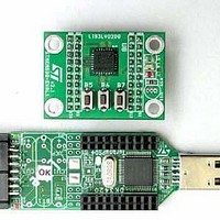
Manufacturer Part Number
STEVAL-IFS001V1
Description
EVAL BOARD 3AXIS MEMS ACCELLRMTR
Manufacturer
STMicroelectronics
Series
MEMSr
Datasheets
1.STEVAL-IFS001V1.pdf
(42 pages)
2.STEVAL-IFS001V1.pdf
(14 pages)
3.STEVAL-IFS001V1.pdf
(4 pages)
4.STEVAL-IFS001V1.pdf
(14 pages)
Specifications of STEVAL-IFS001V1
Design Resources
STEVAL-IFS001V1 Gerber Files STEVAL-IFS001V1 Schematic STEVAL-IFS001V1 Bill of Material
Sensor Type
Accelerometer, 3 Axis
Sensing Range
±2g, 6g
Interface
I²C, SPI
Sensitivity
1024 LSb/g
Voltage - Supply
2.16 V ~ 3.6 V
Embedded
Yes, MCU, 8-Bit
Utilized Ic / Part
LIS3LV02DQ
Processor To Be Evaluated
LIS3LV02DQ
Interface Type
USB
Lead Free Status / RoHS Status
Contains lead / RoHS non-compliant
Other names
497-5069
Available stocks
Company
Part Number
Manufacturer
Quantity
Price


7 Register Description
7.10
28/42
trimmed and they are different for every accelerometer. They permit a good behavior of the
device and normally they have not to be changed. At the end of the boot process the BOOT bit
is set again to ‘0’.
IEN bit is used to switch the value present on data-ready pad between Data-Ready signal and
Interrupt signal. At power up the Data-ready signal is chosen. It is however necessary to modify
DRDY bit to enable Data-Ready signal generation.
DRDY bit is used to enable Data-Ready (RDY/INT) pin activation. If DRDY bit is ‘0’ (default
value) on Data-Ready pad a ‘0’ value is present. If a Data-Ready signal is desired it is
necessary to set to ‘1’ DRDY bit. Data-Ready signal goes to ‘1’ whenever a new data is
available for all the enabled axis. For example if Z-axis is disabled, Data-Ready signal goes to
‘1’ when new values are available for both X and Y axis. Data-Ready signal comes back to ‘0’
when all the registers containing values of the enabled axis are read. To be sure not to loose
any data coming from the accelerometer data registers must be read before a new Data-Ready
rising edge is generated. In this case Data-ready signal will have the same frequency of the
data rate chosen.
SIM bit selects the SPI Serial Interface Mode. When SIM is ‘0’ (default value) the 4-wire
interface mode is selected. The data coming from the device are sent to SDO pad. In 3-wire
interface mode output data are sent to SDA_SDI pad.
DAS bit permits to decide between 12 bit right justified and 16 bit left justified representation of
data coming from the device. The first case is the default case and the most significant bits are
replaced by the bit representing the sign.
CTRL_REG3 (22h)
FDS bit enables (FDS=1) or bypass (FDS=0) the high pass filter in the signal chain of the
sensor
CFS1, CFS0 bits defines the coefficient Hpc to be used to calculate the -3dB cut-off frequency
of the high pass filter:
ECK
HPDD
HPFF
FDS
CFS1, CFS0
External Clock. Default value: 0
(0: clock from internal oscillator; 1: clock from external pad)
High Pass filter enabled for Direction Detection. Default value: 0
(0: filter bypassed; 1: filter enabled)
High Pass filter enabled for Free-Fall and Wake-Up. Default value: 0
(0: filter bypassed; 1: filter enabled)
Filtered Data Selection. Default value: 0
(0: internal filter bypassed; 1: data from internal filter)
High-pass filter Cut-off Frequency Selection. Default value: 00
(00: Hpc=512
01: Hpc=1024
10: Hpc=2048
11: Hpc=4096)
ECK
HPDD
HPFF
f
cu toff
CD00047926
FDS
=
0.318
-------------- - ODRx
Hpc
res
⋅
---------------- -
2
res
CFS1
CFS0
LIS3LV02DQ
Related parts for STEVAL-IFS001V1
Image
Part Number
Description
Manufacturer
Datasheet
Request
R

Part Number:
Description:
BOARD EVAL SPZB260 MOD FOR STR9
Manufacturer:
STMicroelectronics
Datasheet:

Part Number:
Description:
BOARD EVAL EXTENSION SN250
Manufacturer:
STMicroelectronics
Datasheet:

Part Number:
Description:
BOARD EVAL AB-54003L-512
Manufacturer:
STMicroelectronics
Datasheet:

Part Number:
Description:
BOARD REF DESIGN RF DMOS PWR AMP
Manufacturer:
STMicroelectronics
Datasheet:

Part Number:
Description:
BOARD EVAL PWR AMP AB-84008L-470
Manufacturer:
STMicroelectronics
Datasheet:

Part Number:
Description:
BOARD EVAL FOR STM32F103XX
Manufacturer:
STMicroelectronics
Datasheet:

Part Number:
Description:
BOARD EVAL AB-54003L-512
Manufacturer:
STMicroelectronics
Datasheet:

Part Number:
Description:
BOARD SMART PLUG STM32 SPZB260PR
Manufacturer:
STMicroelectronics
Datasheet:

Part Number:
Description:
BOARD DEMO BLUETOOTH SPBT2532C2
Manufacturer:
STMicroelectronics
Datasheet:
Part Number:
Description:
ZIGBEE USB DONGLE EVAL KIT
Manufacturer:
STMicroelectronics
Datasheet:
Part Number:
Description:
STMicroelectronics [RIPPLE-CARRY BINARY COUNTER/DIVIDERS]
Manufacturer:
STMicroelectronics
Datasheet:
Part Number:
Description:
STMicroelectronics [LIQUID-CRYSTAL DISPLAY DRIVERS]
Manufacturer:
STMicroelectronics
Datasheet:

Part Number:
Description:
BOARD EVAL FOR MEMS SENSORS
Manufacturer:
STMicroelectronics
Datasheet: